Metal Oxide Semiconductor FETS
Metal-oxide semiconductor field-effect transistors (MOSFET) are used in the EV industry as Silicon Carbide switches. These devices are highly efficient, fast switching, vertical platforms with minimal losses; properties that make them small, cheap, efficient, but also quite hot.
Even though traditional Power modules mainly use IGBT devices, electric vehicles have space limitations that require smaller, power-denser solutions to accommodate the power control unit. And that's where SiC MOSFETs come in. But with great power come great thermal dissipation needs so the main focus on these new packages is the thermal performance that allows for both high power density and stable operational conditions.
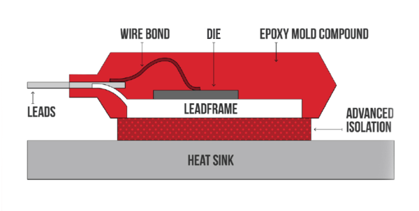
In order to achieve proper cooling, we need to rely on new package designs, molding compounds for high thermal applications, alternative wire-bonding designs and high-end thermal interface materials. These package setups are the alpha and omega of the inverter design as they determine its final form and size. The entire EV vehicle ecosystem, from the charger to inverter, needs to be perfectly designed so that it can pack as much punch as possible to as little space. All the while making sure that safety and operations are still kept to high standards with great thermal dissipation and electrical requirements.
In order to achieve proper cooling, we need to rely on new package designs, molding compounds for high thermal applications, alternative wire-bonding designs and high-end thermal interface materials. These package setups are the alpha and omega of the inverter design as they determine its final form and size. The entire EV vehicle ecosystem, from the charger to inverter, needs to be perfectly designed so that it can pack as much punch as possible to as little space. All the while making sure that safety and operations are still kept to high standards with great thermal dissipation and electrical requirements.
Transistor outline packages such as TO-220 or TO-247 can comfortably house a SiC switch and all the power it brings on board. There are multiple arrangements, for this otherwise simple layout, that combined with a SiC die bring minimal switching losses along with fast switching speeds.
To attain this high performance and the resulting high temperatures while still operable, they need molding compounds specifically made for high-temperature operations and not the ones typically used for Si packages. SiC itself is only limited by the sum of the other parts so we need to design an ideal package to support it. Additionally, thermal insulators are needed to optimize the direct connection to the heatsink.
To attain this high performance and the resulting high temperatures while still operable, they need molding compounds specifically made for high-temperature operations and not the ones typically used for Si packages. SiC itself is only limited by the sum of the other parts so we need to design an ideal package to support it. Additionally, thermal insulators are needed to optimize the direct connection to the heatsink.

Source: chargedevs.com
SiC MOSFET devices perform better at high temperatures compared to plain Si or GaN. 1200V MOSFETs deliver power density and switching efficiency at half the cost per amp of previous generation MOSFETs. With this new MOSFET platform, we already have design wins in multiple segments like solar inverters and uninterruptible power supply (UPS) systems.
Due to the rapid acceptance of the latest generation of SiC MOSFETs, companies are shipping pre-production volumes ahead of schedule and ramping volume production in-line with customer demands.
Epoxy molding compounds for SiC MOSFETs
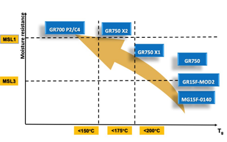
Epoxy molding compounds such as the GR750 series and GR15F-MOD2C are made with power modules in mind. With exquisite thermal performance these compounds have a very high Glass transition temperature and easy pass HTRB tests while keeping high MSL levels. They are designed for high power devices with low moisture absorption and are advancing the technology to meet higher MSL levels requirements.
Hysol GR15F-MOD2C is a High Tg (235°C) molding compound, qualified and in use for 2nd generation SiC MOSFET from the world’s leading manufacturer of Silicon Carbide based diodes for POWER control and management.
Hysol GR15F-MOD2C is a High Tg (235°C) molding compound, qualified and in use for 2nd generation SiC MOSFET from the world’s leading manufacturer of Silicon Carbide based diodes for POWER control and management.

SiC MOSFETS require excellent thermal, electrical and reliability properties in order to pass thermal, HTRB and MSL tests.
Excellent Thermal Stability (Thermal cycling test)
- High Tg as required
- Low weight loss by TGA test and low thermal expansion
Excellent Electrical Stability (HTRB test)
- Low ion content and low ionic mobility at high power condition
- Stable ionic conductivity and permittivity at high temperature condition;
Reliability for SiC MOSFETs Packages (MSL test)
- Low moisture absorption
- Low storage modulus
- Superior adhesion to lead frame
- Low Coefficient of Thermal Expansion (CTE)
Environmentally Friendly
- Green material without Br/Sb comply with RoHS;
- Suitable for halogen-free devices defined by the Jedec JS709B;
Product development map


