High Purity Alumina
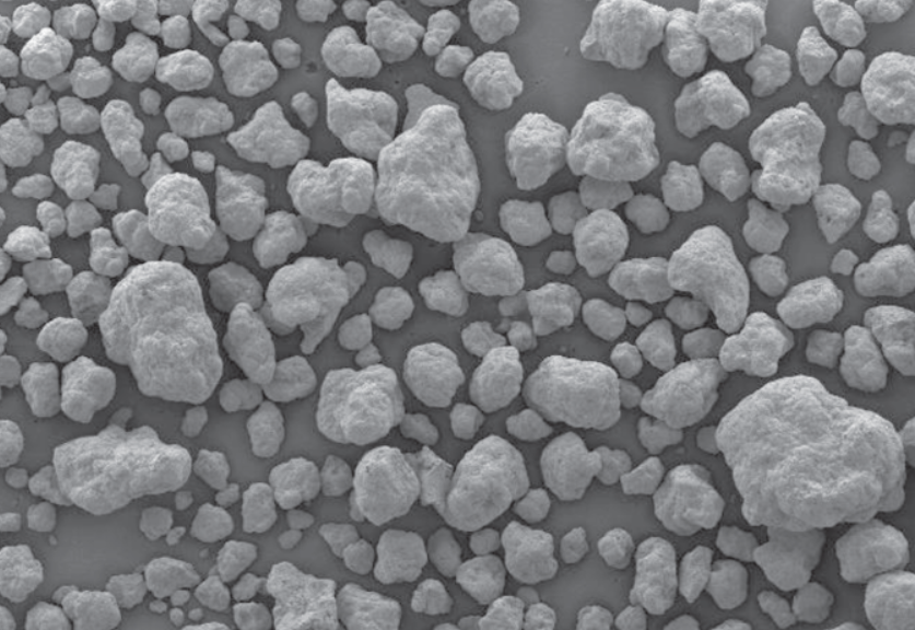
High Purity Alpha Alumina Powder is engineered to meet exacting standards of purity and consistency, crucial for advanced applications in sectors such as semiconductors, technical ceramics, and electronics. Available in varying grades (3N, 4N, 5N) that denote purity levels from 99.9% to 99.999%, this alumina powder features controlled particle size distribution, tailored specific surface areas, and minimal impurities, making it ideal for applications requiring high thermal conductivity and electrical insulation properties.
These characteristics are crucial in enhancing the performance and compatibility of the material within different industrial processes. For instance, in semiconductor manufacturing, a consistent particle size distribution ensures uniformity and reliability in insulating layers. Similarly, in technical ceramics, tailored specific surface areas can significantly impact the material's sintering behavior and final mechanical strength. Furthermore, the powder's minimal impurity content minimizes the risk of contamination and defects, thereby improving the overall quality and longevity of the end products. This makes High Purity Alpha Alumina Powder an indispensable material for cutting-edge technological applications where precision and reliability are paramount.
TECHGuard 4045S | 4N Purity Spherical Alumina
- 4N Purity (99.99%)
- 0.3 - 0.55um particle size
- Coatings, aerospace parts, medical ceramics
- 12 weeks
TECHGuard 4170P | 4N Purity Irregular Alumina
- 4N Purity
- 1.4 - 2.0um particle size
- Coatings, aerospace parts, medical ceramics
- 12 weeks
TECHGuard 4065S | 4N Purity Spherical Alumina
- 4N Purity (99.99%)
- 0.55 - 0.8 um particle size
- Coatings, aerospace parts, medical ceramics
- 12 weeks
TECHGuard 4120P | 4N Purity Irregular Alumina
- 4N Purity (99.99%)
- 1.0 - 1.4 um particle size
- Coatings, aerospace parts, medical ceramics
- 6 weeks
CRYSTALGuard 4360Q | 4N Purity Alumina Pucks
- 4N purity (99.99%)
- Puck form
- Ideal for sapphire applications
- 12 weeks
PUREGuard 5120P | 5N Purity Irregular Alumina
- 5N purity (99.999%)
- 1.0 - 1.4um particle size
- Ideal for Semiconductor manufacturing
- 6 weeks
PUREGuard 5065S | 5N Purity Spherical Alumina
- 5N purity (99.999%)
- 0.55 - 0.8um particle size
- Ideal for semiconductor manufacturing
- 12 weeks
PUREGuard 5045S | 5N Purity Spherical Alumina
- 5N purity (99.999%)
- 0.3 - 0.55um particle size
- Ideal for semiconductor manufacturing
- 12 weeks
PUREGuard 5170P | 5N Purity Irregular Alumina
- 5N purity (99.999%)
- 1.4 - 2.0um particle size
- Ideal for Semiconductor manufacturing
- 12 weeks
CRYSTALGuard 5360Q | 5N Purity Alumina Pucks
- 5N purity (99.999%)
- Puck form
- Ideal for Sapphire Applications
- 12 weeks
Product Selector Guide
| Product Code | Units | 4045S | 4065S | 5045S | 5065S |
| Purity | — | 4N | 4N | 5N | 5N |
| Crystal Phase | — | alpha | alpha | alpha | alpha |
| Morphology | — | spherical | spherical | spherical | spherical |
| BET | m2/g | 6-10 | 6-10 | 6-10 | 6-10 |
| Primary Particle Size | µm | 0.3-0.55 | 0.55-0.8 | 0.3-0.55 | 0.55-0.8 |
| Na | ppm | 30 | 30 | 10 | 10 |
| Si | ppm | 12 | 12 | 8 | 8 |
| Fe | ppm | 10 | 10 | 5 | 5 |
| Ca | ppm | 8 | 8 | 5 | 5 |
| Product Code | Units | 4120P | 4170P | 5120P | 5170P |
| Purity | — | 4N | 4N | 5N | 5N |
| Crystal Phase | — | alpha | alpha | alpha | alpha |
| Morphology | — | irregular | irregular | irregular | irregular |
| BET | m2/g | 4-7 | 4-7 | 4-7 | 4-7 |
| PSD (D50) | µm | 1.0-1.4 | 1.4-2.0 | 1.0-1.4 | 1.4-2.0 |
| Loose Density | g/cm3 | 0.3-0.5 | 0.3-0.5 | 0.3-0.5 | 0.3-0.5 |
| Na | ppm | 30 | 30 | 10 | 10 |
| Si | ppm | 12 | 12 | 8 | 8 |
| Fe | ppm | 10 | 10 | 5 | 5 |
| Ca | ppm | 8 | 8 | 5 | 5 |
| Product Code | Units | 4360Q | 5360Q |
| Purity | — | 4N | 5N |
| Crystal Phase | — | alpha | alpha |
| Format | — | puck | puck |
| Field Density | g/cm3 | >3.4 | >3.4 |
| Average Dimensions (L, W, H) | mm | 59,59,39 | 59,59,39 |
| Average Mass | g | 450 | 450 |
| Na | ppm | 30 | 5 |
| Si | ppm | 10 | 6 |
| Fe | ppm | 8 | 5 |
| Ca | ppm | 8 | 4 |
Frequently Asked Questions
What is Alumina?
Alumina, or aluminum oxide (Al2O3), is a white crystalline powder that is produced from bauxite through the Bayer process. It is used as a raw material in the production of aluminum metal and has numerous industrial applications due to its hardness and resistance to wear and corrosion.
How is Alumina produced?
Alumina is produced through the Bayer process, which involves refining bauxite ore to obtain aluminum oxide. Bauxite is first crushed and mixed with caustic soda, which dissolves the alumina. The solution is then filtered to remove impurities, and the alumina is precipitated out, washed, and heated to remove water.
What are the main applications of Alumina?
Alumina is widely used in various industries. Its primary use is in the production of aluminum metal. It is also used in the manufacture of ceramics, refractories, abrasives, and as a filler in plastics and cosmetics. Additionally, alumina is used in water purification and as a catalyst in chemical processes.
Does Alumina still being used in Chemical Mechanical Polishing (CMP)?
Alumina is used for polishing silicon carbide by companies like Wolfspeed and STMicroelectronics. While some have shifted to softer particles like silica, alumina is still required for higher material removal rates.
Learn More
What is the key element concentration of Alumina purities?
| Purity | Na | Mg | Si | Ca | Ti | Cu | Cr | Fe | K |
| 3N (99.9%) | <150 | <20 | <50 | <50 | <20 | <10 | <5 | <50 | <20 |
| 4N(99.99%) | <30 | <5 | <10 | <10 | <5 | <5 | <5 | <20 | <10 |
| 5N(99.999%) | <4 | <1 | <3 | <3 | <0.5 | <0.5 | <1 | <1 | <0.5 |
What is High purity alumina?
High purity alumina (HPA) is essential in semiconductor leading-edge devices due to the significant challenges posed by impurities. These impurities can be difficult to measure accurately during processing or within components before they are utilized in manufacturing. This makes the need for higher purity materials, particularly in etch processes, critically important.
HPA that is 99.99% pure, as opposed to the more common 99.8%, offers several advantages. Firstly, it promises lower copper and iron contamination, which is crucial for enhancing device reliability. Copper and iron impurities can degrade device performance and longevity, so reducing these contaminants is key to maintaining high-quality standards. Additionally, lower SiO2 content in HPA helps to minimize particulate contamination, which can adversely affect the manufacturing process and the final product's integrity.
Moreover, lower soda and calcium content in HPA are correlated with a lower loss tangent, which is beneficial for applications where RF energy is transmitted through a ceramic component inside a wafer chamber. This property is crucial for maintaining efficient and effective RF transmission, thereby improving the overall performance of semiconductor devices.
Feedback from one of the leading semiconductor OEMs highlights that the dielectric constant and strength of our HPA are superior to those of other UHPA manufacturers. This superior performance underscores the importance of using high purity alumina in achieving the highest standards in semiconductor manufacturing, ensuring better device reliability, minimized contamination, and enhanced performance in RF applications.
Comparison of High Purity Alumina (HPA) and Ultra High Purity Alumina (UHPA)
| Attribute | High Purity Alumina (HPA) | Ultra High Purity Alumina (UHPA) |
|---|---|---|
| Purity Level | 3N (99.9%), 4N (99.99%), 5N (99.999%) | > 5N (99.999%) |
| Typical Applications |
|
|
| Main Properties |
|
|
| Environmental Impact | Industry standard production methods | Environmentally sustainable production with significant reduction in greenhouse gas emissions and power consumption |
| Reliability and Quality |
|
|
| Notable Feedback | Widely accepted in various advanced applications | Positive feedback from leading semiconductor OEMs regarding dielectric constant and strength superiority |
What is Ultra High Purity Alumina?
Ultra High Purity Alumina (UHPA) is critical for advanced applications where even minute impurities can cause significant issues. The superior quality of UHPA, characterized by purity levels greater than 99.999% (5N), ensures exceptional performance and reliability in the most demanding industries. Here are key reasons why ultra high purity matters:
One of the most critical attributes of UHPA is its superior dielectric performance. This makes UHPA an ideal material for electronic applications where high dielectric strength is necessary. The ultra high purity ensures minimal electrical losses and higher efficiency, which is particularly important in high-frequency and high-power devices. The absence of impurities like soda and calcium further enhances the material's dielectric properties, making it a preferred choice for advanced electronic components.
Semiconductors:
In semiconductor manufacturing, contamination such as metal ions, particles, and organic residues can create device-level “killer defects” that significantly impact yield and performance. Contamination accounts for over 75% of the yield losses in semiconductor (IC) device manufacturing. UHPA, with its extreme purity, minimizes the risk of such contamination, thereby improving the reliability and efficiency of semiconductor devices. This leads to higher yield rates, lower production costs, and more reliable end products.
Sapphire Production:
For sapphire production, particularly in applications like LEDs and other electronic devices, the high purity level of UHPA is crucial. Trace impurities in the alumina can significantly affect the performance and efficiency of sapphire products. UHPA ensures that the sapphire produced is of the highest quality, with optimal optical clarity and mechanical strength. This translates to better performance and longer life for sapphire-based components in high-tech applications.
Phase Transformation of Alumina
Alumina has a complex structure and many crystalline polymorphic phases such as α-Al2O3, βAl2O3, γ-Al2O3, δ-Al2O3, θ-Al2O3, η-Al2O3, κ-Al2O3, χAl2O3 and ρ-Al2O3. The phase transition temperatures are different for different precursors during their calcination as shown in Figure:
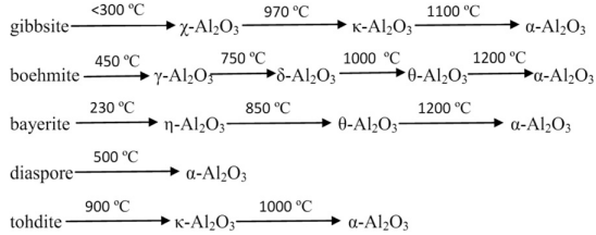
Among the numerous crystal forms of alumina, α-Al2O3 and γ-Al2O3 are the two most common kinds. α-Al2O3 has some excellent physical and chemical properties such as good acid, alkali and heat resistances and high hardness and strength. It is widely used in different fields such as ceramics, surface protective layer materials, refractory materials, catalysts and catalyst supports and optical materials. γ-Al2O3, which is also called activated alumina, has a large surface area, strong adsorption capacity, good catalytic activity and wear resistance. It is also widely applied in various fields such as adsorbents, ceramics, catalysts and catalyst supports.
Different Morphological Shapes of Alumina
The application performance of alumina depends on not only the size of ultra-fine particles but also the particle shape. Alumina has a variety of shapes such as rod, fibrous structure, flake, and sphere. Different shapes of alumina have different physical and chemical properties and applications. For example, the fibrous nano-alumina has a very strong antisintering property, which is often used as an additive for epoxy resin to improve its tensile strength and rigidity. The flake-like alumina is generally used as a seed crystal added to ceramics, which significantly enhances the toughness of ceramics.
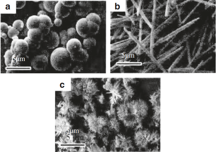
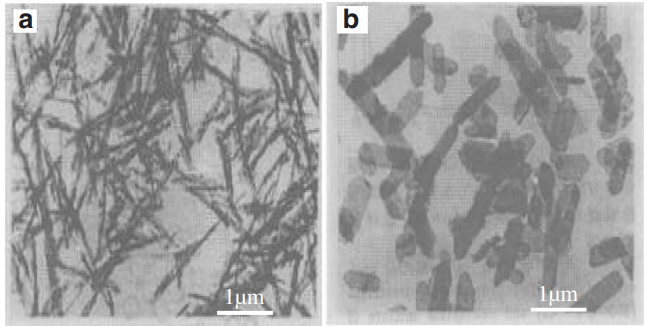
TEM image of alumina prepared under different synthetic temperatures producing different shapes. (A) 90 °C (Spherical) (B) 120 °C (Fibrous) (C) 150 °C flaky | TEM image of α-Al2O3. (A) Needle-like α-Al2O3. (B) Plate-like α-Al2O3 |

Table: Effect of calcination temperature on the size of alumina
in the presence of additives
The morphology of Al2O3 can be influenced by various factors such as raw materials, concentrations, different synthesis methods, additives and heat treatment system. During the preparation of Al2O3, the morphology of the precursors and the protection of the particles during heat treatment play a decisive role in the final morphology of alumina. The morphology will not change during the low-temperature heat treatment. However, when high temperature is reached, the diffusion of the powder particles accelerates. Thus, the particles diffuse from the inside to the surface of the crystal lattice and spread to the surrounding resulting in the neckformation as well as the agglomeration of surrounded particles. Accordingly, the morphology of the particles changes. The use of various additives effectively reduces the calcination temperature; consequently, the problem of particle agglomeration can be solved. The utilization of template is a new research hotspot with the objective of improving the dispersibility of Al2O3 powder and controlling the shape of the sample particles.
High Purity Alumina Markets & Applications

Semiconductor
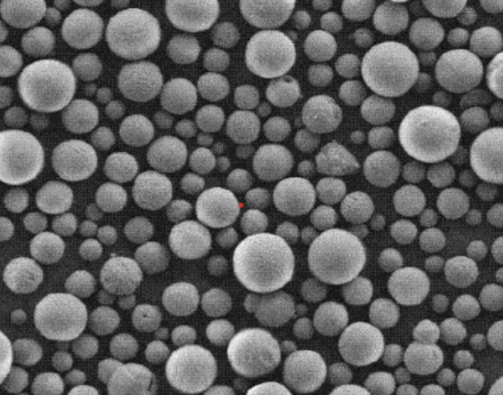
Our high purity alumina helps make next-generation technology possible by providing consistent quality 5N purity critical to the end user applications. 5N purity has lower contaminates/impurities and higher performance. High Purity Alumina (HPA) is preferred for standard semiconductor applications, whereas Ultra High Purity Alumina (UHPA) is essential for leading-edge technologies where even the smallest impurity can cause significant issues.
Thermal Interface Materials
Polar Performance Materials manufactures HPA for use in high-end applications like EMC for the emerging AI/HBM (high bandwidth memory) application. The combination of high thermal conductivity, stability, chemical inertness, and electrical insulation makes High Purity Alumina an excellent choice for high-end thermal applications. UHPA is preferable for applications requiring maximum thermal management and minimal contamination.

Aerospace and Defense
Our specially-designed 4N-5N powders are critical to aerospace and defense as purity becomes more important. Applications include chemical & corrosion resistance, optical components, coatings & thermal barriers, insulators, and electrical components. HPA is suitable for general applications, while UHPA is essential for critical components where failure is not an option due to its superior purity and performance.

Sapphire
Our 5N purity highly densified pucks are critical to high-quality sapphire used in the Semiconductor industry, LED, and other electronic applications. UHPA is crucial for producing sapphire substrates used in high-performance electronics and optics, ensuring minimal defects and high efficiency.
Technical Ceramics
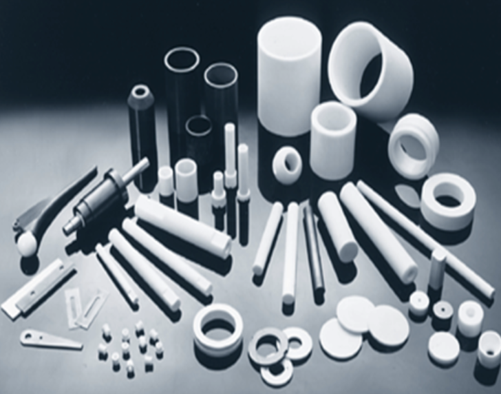
Increased chemical resistance, products made of HPA have lower impurities and higher dielectric performance. This accounts for an increase in mechanical strength. Both HPA and UHPA are used, with UHPA preferred for applications demanding the highest mechanical strength and purity, such as in high-stress environments or where electrical insulation is paramount.

Batteries
High Purity Alumina Manufacturing
Tailored Purity Levels
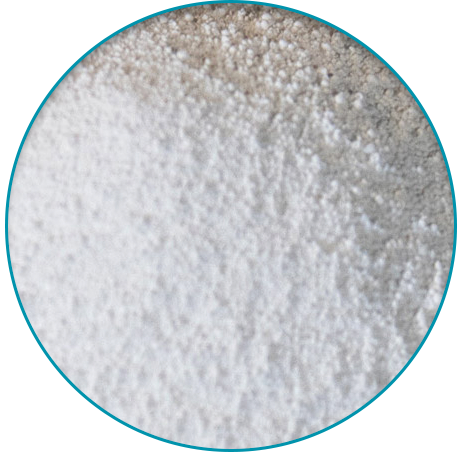
Offering varying purity levels such as 3N (99.9%), 4N (99.99%), and 5N (99.999%) allows for customization to meet the specific needs of diverse industries, including semiconductors, technical ceramics, and high-precision manufacturing. The precise control over impurity levels ensures that each application receives the appropriate material quality, which is critical in achieving optimal performance and reliability. For example, the semiconductor industry demands extremely high purity to prevent any electrical interference and ensure device longevity, whereas technical ceramics may require specific impurity profiles to enhance mechanical properties. Our ability to tailor purity levels guarantees that our materials meet the stringent requirements of these advanced applications.
Tailored Particle Size Distributions and Specific Surface Areas
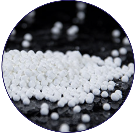
The ability to customize particle size distributions and specific surface areas is essential in meeting the unique demands of various applications. For instance, smaller particle sizes with higher surface areas are often preferred in catalysis and battery technologies for their enhanced reactivity and efficiency. Conversely, larger particles may be advantageous in structural ceramics for improved mechanical strength. By precisely controlling these parameters, we can optimize the performance, compatibility, and overall effectiveness of the material in its intended application. This customization enhances not only the functional properties but also the processing characteristics, such as flowability and compaction behavior, ensuring seamless integration into customer processes.
Advanced Manufacturing
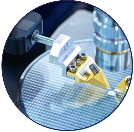
Utilizing state-of-the-art processing technology is crucial in maintaining unparalleled consistency and quality across our product range. Advanced manufacturing techniques, such as precision milling, controlled atmosphere furnaces, and high-purity gas systems, ensure that each batch of material meets the exacting standards required by high-tech industries. This commitment to advanced manufacturing allows us to produce materials with uniform particle size distributions, controlled surface chemistries, and minimal contamination, which are essential for applications in semiconductors, optics, and other high-precision fields. The integration of real-time monitoring and quality control systems further ensures that every product consistently meets the highest quality benchmarks.
Customizable Solutions
We offer customizable solutions by adapting properties and incorporating specific additives to fit precise customer applications, thereby enhancing product functionality. This includes modifying chemical compositions, particle morphologies, and incorporating dopants or stabilizers to achieve desired characteristics. For example, adding specific dopants to semiconductor materials can tailor electrical properties, while incorporating stabilizers in ceramic materials can improve thermal and mechanical stability. Our customizable solutions are developed in close collaboration with customers, ensuring that the final product perfectly aligns with their technical requirements and performance goals. This flexibility not only meets the immediate needs but also anticipates future advancements in technology and application demands.
Particle Size Distribution: Key factor for performance, typically ranging from 1 to 5 microns, with some sampling down to 0.07 microns
Densification Process: Improves product characteristics, including theoretical density, which can reach up to 3.9 for technical ceramics.

Expert Support
Dedicated technical support and collaborative R&D partnerships are central to optimizing application outcomes for our customers. Our team of experts works closely with clients to understand their specific needs and challenges, providing tailored recommendations and technical guidance throughout the product lifecycle. Collaborative R&D efforts drive innovation, enabling the development of cutting-edge materials and solutions that address emerging industry trends and requirements. This partnership approach not only enhances product performance but also accelerates time-to-market for new technologies. Our comprehensive local support includes material characterization, application testing, and process optimization, ensuring that our customers achieve the best possible results with our products.
Sustainable Practices
Our commitment to sustainable practices is reflected in our eco-friendly manufacturing processes that significantly reduce energy consumption and carbon emissions. By leveraging advanced production technologies, such as low-energy milling and recycling of process gases, we minimize environmental impact while maintaining high product purity and quality. This approach not only supports global sustainability initiatives but also enhances the efficiency and cost-effectiveness of our manufacturing processes. Our process requires 7 steps to refine alumina, significantly fewer than competitors like Sumitomo, which require 20-27 steps. This streamlined process results in lower energy consumption and higher sustainability Our patented technology uses 40%- 75% less energy than competitive processes. We produce 90-98% less emissions than competitive processes, given our Ontario Canada location which utilizes hydroelectric power of Niagara Falls. Another competitive edge we have on our process is unlike other manufacturers, the process does not create harmful waste such as "wet mud" only saltwater as a byproduct.
Sustainable practices extend to our supply chain management, where we prioritize sourcing raw materials from environmentally responsible suppliers and optimize logistics to reduce our carbon footprint. These efforts ensure that our products contribute to a more sustainable future without compromising on performance or reliability.

Reliable Supply Chain
We maintain a reliable supply chain with strong logistical capabilities to ensure dependable delivery and consistent product availability. Our NA location ensures business continuity and reduces any supply chain risks. Our robust logistics network, combined with strategic inventory management, allows us to meet customer demands promptly and efficiently, even during periods of high demand or supply chain disruptions. This reliability is backed by our commitment to customer satisfaction and support, ensuring that our clients can rely on us as a trusted partner in their production processes. Our global distribution network ensures that materials reach their destination in optimal condition, while our proactive communication and support services address any issues swiftly, maintaining the highest levels of customer trust and satisfaction.
Presentations
High Purity Alumina for Batteries
The presentation shown on the left is focused on explaining the major costs involved ...


