Printed Circuit Boards (PCBs)
What is a PCB?
A PCB or Printed Circuit Board is an electronic assembly used in almost every modern electronic device. It is a multi-layered component that uses copper tracing to create communication pathways. Through these pathways, electricity travels to the various components that are mounted onto the surface of the PCB.
How is a PCB Manufactured?
Generally, PCB manufacturing varies greatly based on the type of PCB and manufacturing techniques. PCBs typically start out as a copper-clad laminate, which is then fused to an insulating substrate made of fiberglass-reinforced epoxy, commonly known as FR-4. The PCB design and pathways are created through specialized PCB design software, and then the design is generated and used to guide the manufacturing process. It is then dipped in a chemical bath which etches away the copper in the design not covered by the stencil so that when the stencil is removed the copper conductive traces remain.
After many processing and inspection steps, electronic components like resistors and capacitors are soldered to the board. To create functional circuits, the leads are connected to the conductive traces. Then, a silkscreen layer is printed on top of the board, which contains text and symbols that act as identifiers for the different components.
Finally, the sheet is covered in a solder mask, protecting the board from corrosion and debris. This mask is what gives the PCB its characteristic green color, however, solder masks also come in colors like blue or black. Most importantly, solder masks are what provide the board with electrical insulation.
What is a Flexible PCB?
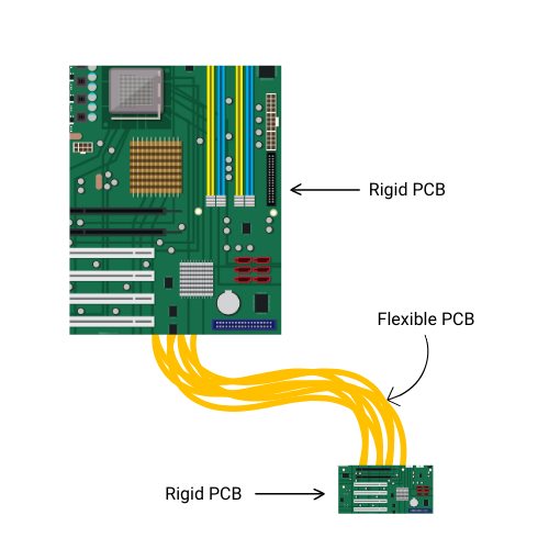
A category of PCBs is a flex PCB. As the name suggests, this printed circuit board is made with flexible materials, opening up more opportunities for use in constrained areas where flexibility is required. Like a rigid PCB, the flex PCB contains copper tracing communications pathways. The main difference is that instead of a rigid fiberglass-reinforced epoxy substrate, flex PCBs are made with a non-conductive polymer substrate like polyimide or polyester.
Manufacturing a PCB with these materials makes it bendable and light, which can be extremely beneficial in applications where there are space constraints or weight requirements.
In some cases, rigid and flex PCBs are combined to create a rigid-flex PCB. This is a hybrid circuit board that combines both technologies to create a customizable PCB, which can be very fitting to specific applications where rigidity but also flexibility is required.
PCB Assembly Process Flow
PCB assembly is a manufacturing process that involves attaching electronic components to a printed circuit board (PCB). It typically begins with a bare PCB and progresses through several stages including component placement, soldering, and inspection to create a functional electronic product.
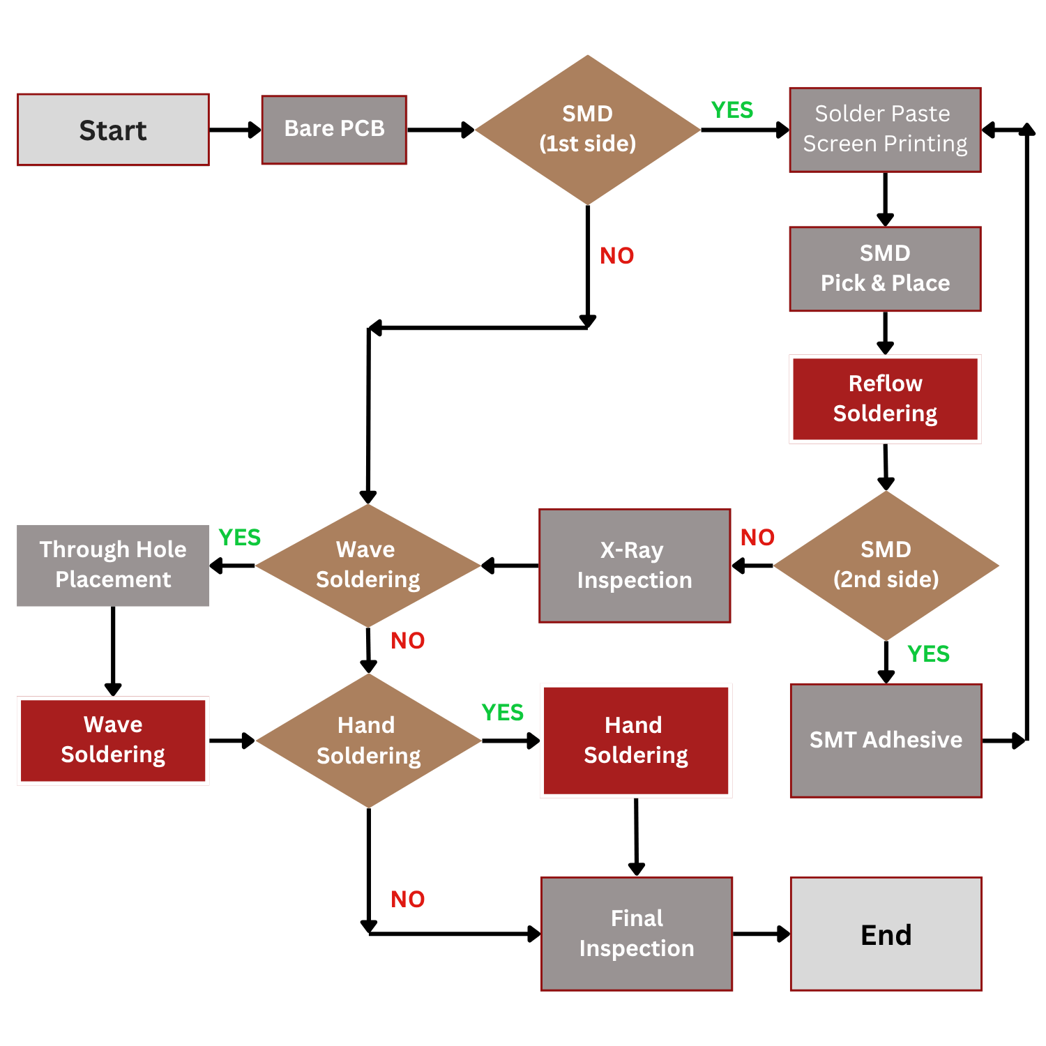
The process starts with thoroughly inspecting the bare PCB to ensure it meets the design specifications and is free of defects. On the PCB board, a stencil with openings corresponding to SMD (surface mount device component) component pads is placed. Solder paste, a viscous mixture containing solder particles and flux, is applied through the stencil onto the designated pads where SMD components will be placed. After applying the solder paste, the solder paste on the PCB board will then be inspected using the solder paste inspection (SPI) machines.
Automated machines precisely pick up surface mount components (SMDs) and place them onto the PCB pads with the solder paste. The PCB is conveyed through a reflow oven. Controlled heating melts the solder paste, creating strong electrical and mechanical connections between the components and the PCB pads. The assembled PCB is carefully flipped over to access the second side and the process is repeated from the solder paste application using a stencil, component placement and the PCB undergoes the reflow soldering process again to create solder joints on the second side.
After reflow, the PCB is cleaned to remove any residual flux, a cleaning agent used in the soldering process. For some designs, components with leads are inserted through designated holes in the PCB. For through-hole components, the PCB is passed over a wave of molten solder, creating solder joints on both sides of the board. It's also common to add individual components after the main assembly process using conventional hand soldering. The assembled PCB then undergoes a rigorous visual inspection and automated optical inspection (AOI) to detect any defects including misalignment, missing components, and solder issues. The final stage involves electrical testing to ensure the assembled PCB functions as designed.
Presentations
The evolution from lead-containing Sn63Pb37 wire to Pb-free micron-sized Solder Spheres
The evolution of Printed Circuit Boards and Semiconductors have also forced solder technology to evolve from through-hole and solder baths to surface mounted with solder paste, and now finally solder spheres for BGAs, and flip chips.
Semiconductors and printed circuit board technology are relentlessly evolving industries. Their constant development has forced solder technolgy to change and evolve too. Solder technology, as a whole, has moved from lead-based solder wire and separately applied solder flux to solder spheres. The latest industry break-through being a move away from wire bonding to micron size solder spheres for flipchips. To understand how this happened let\'s start by breaking down the product name Sn63Pb37 into its parts:
Sn = Tin
63 = 63%
Pb = Lead
37 = 37%
Alloys melt at different temperatures based on their composition or ratio of metals. Sn63Pb37 solder liquifies at exactly 183°C. Because the liquidus phase is so perfectly defined, Sn63Pb37 is known as a eutectic solder. This is very useful for two reasons. The first is that there is no "slurry phase" as some of the metals melt and others have not yet melted. The second is that the 183°C temperature is incredibly useful for circuit boards because it was high enough to melt the solder but low enough not to damage plastic components or the circuit board itself.
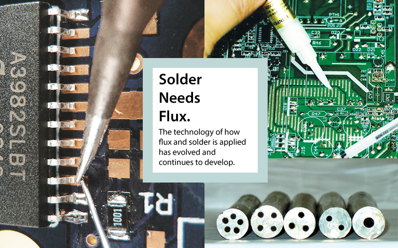
Solder wire needs flux. Flux removes oxidation.
Without flux the layer of oxidation acts as a barrier between the solder and the two conductive contact points thus preventing a clean and solid solder joint.
Pre-coating parts in flux was, therefore, an essential extra step that cost more time and labor. So the next step in solder development was hollow solder wire filled with an internal flux. Further developments included multi-core wire with multiple hollows for better distribution of flux.
The industrial mass-produced Printed Circuit Board (PCB), as we know it, started out with through-hole technology. Semiconductor devices and chips had pins which were pushed through holes in the printed circuit board. The bottom side of the entire circuit board would then have flux applied in one go and then be dipped into a solder bath. This automated the soldering process and eliminated unnecessary extra steps. Which, in terms of mass production, saved millions of dollars in energy and material.
Evolving ICs – Pushing soldering technology to evolve
After through-hole technology PCBs evolved towards surface mounted technology: where solder paste was used. Solder paste is a suspension of powdered flux and powdered solder together. This allowed solder to be printed on circuit boards by a solder paste printer and then melted in one go in a solder reflow process: thereby allowing for much more complex and densely packed installations of semiconductors on the PCB.
Integrated circuits have been getting smaller and smaller and with larger and larger numbers of tiny transistors. This can be best seen in the evolution of Small Outline Integrated Circuits or SOIC: evolving at first by doubling the number of inputs and outputs or pinouts: from SO8, on to SO16, SO32. Eventually for the sake efficiency, instead of two rows of pinouts, all four sides would be used in the Quad Flat Pack (QFP). This also meant that the legs got thinner and thinner and got packed closer and closer together.
Array packaging moved semiconductor packages from wire bonding to Solder Spheres
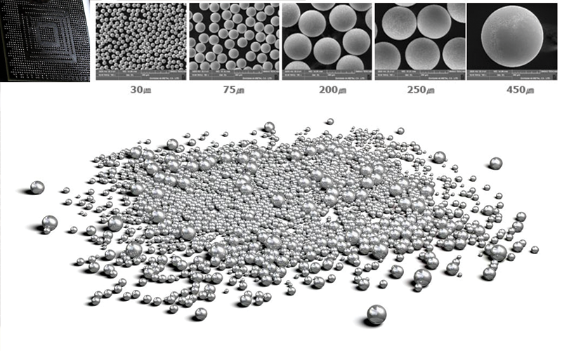
When you are using all four sides and even stacking wafers what can you do to further increase the number of inputs and outputs? The answer turned out to be: use the bottom of the chip as well. So, instead of many small thin legs, solder spheres would be placed directly on the bottom of the chip and would act as the connection between the Ball Grid Array (BGA) and the circuit board. This meant full encapsulation in an epoxy molding compound was no longer necessary and you could simply use an underfill.
250,000 solder spheres: sounds like a lot, but at micron sizes, that’s just enough for a heaped tablespoon full. Eventually, solder spheres got smaller and smaller so that they could pack even tighter grids of connection on the bottom of silica die. In these flip chips setups, tiny solder spheres are used instead of even 25-micron thick gold wire. Solder spheres are made in an amazing process with incredible accuracy and tight quality control.
High Tech Tin
CAPLINQ is not only able to supply the alloys and purify the solder material, but it also has an innovative diameter and spheroid-selecting system of solder balls and an advanced anti-oxidation technology that actually adds an anti-oxidation element to the alloy in addition to its OSP surface coating process.
Not only are our solder spheres High-Tech, but they are made from a unique uniform droplet spraying technology that far outperforms competitors in terms of productivity. This combination of high technology and high productivity allow CAPLINQ to offer its customers the best value for the best product.
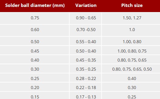
Correlation between solder ball size and BGApitch
A parallel evolution in material: from Lead (Pb) to Lead-free!
Early in the 2000’s in Japan, Sony and other concerned companies started to push for lead-free solder. This was in response to a situation in which electronic devices were ending up in landfills, and these landfills were in turn exposed to rainwater which allowed the lead in the solder to contaminate the groundwater. In 2006 the EU Restriction of Hazard Substances Directive (RoHS) came into effect restricting the use of lead consumer electronics.
This led to SAC305 Lead-free solder replacing eutectic SnPb63/37 solder as the industrial standard: with 75% of companies using it. As a near eutectic solder it has adequate thermal fatigue properties, strength, and wettability. Another advantage of SAC solder is that it’s more resistant to gold-embrittlement and has substantially higher joint strength than PB solders.Going Pb-free however means using silver instead of lead which means increases costs. For some applications SAC solders with less silver are suitable. These include SAC105, Bi57Sn42Ag1, as well as silver-free and lead-free solder , Bi58Sn42.
Using silver means that SAC solders have a 34°C higher melting point than Sn63Pb37 solder at between 217-220°C. This requires a higher solder reflow temperature of 235-245°C in order to achieve wetting and wicking. Some printed circuit components are susceptible to SAC assembly temperatures: including capacitors, optoelectronics etc.
Companies have since started offering 260°C compatible components to meet the high temperature required for SAC solder reflow. 260°C compatibility is fast becoming the new standard for semiconductor and component manufacturers.
Humiseal Conformal Coatings for Printed Circuit Boards
An easy way to protect a PCB and increase its longevity is to apply a Conformal Coating. A conformal coating is a thin film specifically designed to safeguard electronic assemblies. It can protect from dust, corrosion, and moisture, by creating a coating that envelopes the PCB and all its components. Conformal coatings also insulate the PCB, protecting it from electrical failures.
.png)
HumiSeal™ Conformal Coatings are based on different chemistries, including acrylics, silicones, synthetic rubbers, and UV-curable acrylates. Each chemistry offers distinct properties suited for specific application requirements, such as electrical insulation, moisture resistance, chemical protection, or mechanical flexibility. These coatings are also available with varied curing mechanisms (e.g. moisture, heat, UV), allowing compatibility with different production speeds and process constraints.
Featured Products
Excellent chemical resistance
Durable, tough coating
Ideal for harsh environments
Easy apply & rework
Strong moisture resistance
Clear, cost-effective protection
Extreme temperature stability
Flexible & stress-relieving
Excellent moisture protection
Flexible, vibration-resistant
Moisture & salt protection
Easy to repair/remove
Fast UV curing
Clear, moisture-resistant
Ideal for automation
Hard, durable finish
Superior chemical barrier
Strong substrate adhesion
Key Features and Benefits of HumiSealTM Conformal Coatings
- Moisture protection, which prevents corrosion and electrical shorting in electronic assemblies
- Chemical resistance, which safeguards components from harsh environmental contaminants
- Dielectric insulation, which maintains circuit integrity and prevents arcing between conductors
Frequently Asked Questions about Conformal Coatings
The liquid coating “conforms” to every contour of the assembly, creating a continuous protective film that shields components from moisture, dust, chemicals, and electrical leakage.
How do I choose the right conformal coating chemistry?
Selection depends on environmental stresses, thermal range, humidity, mechanical stress, chemical exposure, and reworkability needs. For example:
- Acrylics – easy to apply and rework, limited high-temp resistance
- Silicones – excel in high-humidity, high-temp, vibration-heavy environments
- Polyurethanes – resist solvents and abrasion
- UV-curable – ideal for high-speed, inline production
How is a conformal coating applied?
There are multiple ways to apply a conformal coating, all based on the specifics of the application. Some common methods include:
- Hand Brushing
- Hand Dispensing
- Spray Coating (Aerosol or Handspray)
- Dip Coating
- Selective Coating
Yes. Automated selective coating equipment can precisely deposit coating only on critical areas—leaving connectors, test points, or sockets exposed—reducing masking and cleanup.
What surface preparation is required?
Cleanliness is critical. Assemblies must be free of flux residues, oils, and particulates—often requiring plasma cleaning, ionized air, or aqueous washing. IPC-CC-830 recommends ionic contamination <1.56 µg/cm² NaCl equivalent.
How do coatings perform under thermal cycling and stress?
Performance varies by chemistry:
- Silicones – best for –55 °C to +200 °C cycles, handle vibration without cracking
- Acrylics/Epoxies – may crack or delaminate under extreme flex or rapid thermal change
Featured Presentation: CAPLINQ Product Offerings
CAPLINQ Conformal Coatings for Printed Circuit Boards
Curious about how the right materials can improve PCB Performance? This quick presentation walks you through CAPLINQ’s lineup for Conformal Coatings: what they’re made of, how they perform, and where they fit best. Whether you’re optimizing for efficiency, durability, or both, these materials are engineered to keep up.
Got questions or need help choosing the right materials for your Printed Circuit Boards? Reach out to us!
Contact Us →Presentations
Related Blogs

Mitigating Tin Whiskers in Military and Aerospace Electronics with Conformal Coatings?
This blog discusses tin whiskers in military and aerospace electronics and how they can cause failures. It explains how conformal coatings help mitigate these risks by containing whisker growth and preventing electrical shorts, while highlighting the effectiveness of different coating types.

How to Select the Right Conformal Coating
This blog guides readers through the process of choosing the right conformal coating for electronics. It explains the main coating types (acrylic, urethane, silicone, rubber‑based, UV‑curable), compares their strengths (e.g., temperature resistance, moisture resistance, flexibility), and shows how to match the chemistry to your application needs.
How to Waterproof a PCB with Aculon's PCB Waterproofing Treatments
Certain applications may require waterproofing, such as underwater equipment or electronics like smartphones and watches. In these cases, nanocoatings are a great way to achieve various levels of waterproofing. Aculon's PCB Waterproofing Treatments provide an extremely thin coating that adds hydrophobicity without altering the surface of the PCB. The goal of these treatments is to protect the PCB from short circuits and other damage caused by moisture, which can cause corrosion and degrade the performance of the circuit over time.
Aculon's NanoProof™ Series offers customers a range of PCB waterproofing solutions from protecting against accidental water damage to IPX7, immersion in water at one-meter depth for 30 minutes, to greater barrier properties that can withstand 100 hours of immersion in sweat solutions and some of the most stringent test methods developed for non-hermetic components. Some Waterproofing Treatments Caplinq offers include:
- Nanoproof 1.0 - IPX4, best for a broad range of substrates
- NanoProof 2.1 - best for PCBs and electronic components
Treatments depend on various factors including substrate, hydrophobicity or oleophobicity level, coating thickness, etc.


