- Home

- Products
- Other
- Leadframes
- LINQALLOY ETLF | Etched lead frame
LINQALLOY ETLF | Etched lead frame
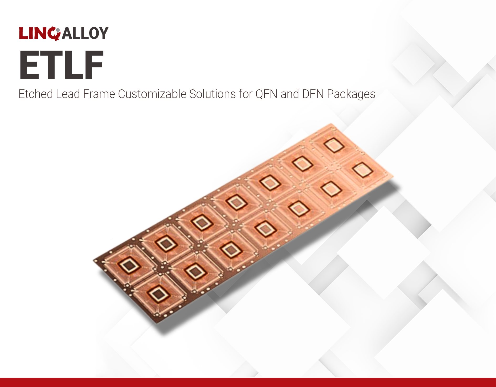

- QFN, DFN
- Package sizes from 1.0mm x 0.6mm to 14mm x 12mm
- Pin count capability from 2 to 156
Product Description
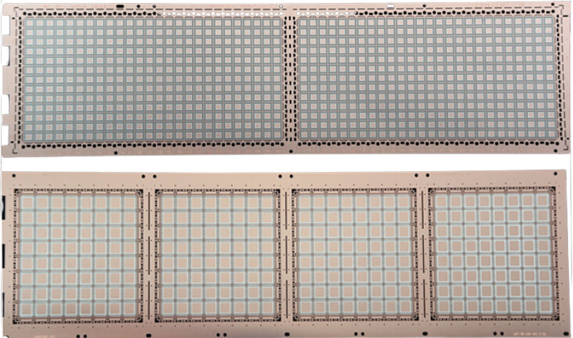
LINQALLOY ETLF Etched lead frames act as the foundation for intricate packages that are essential building compact and powerful devices. It is a flexible lead frame manufacturing which allows for the implementation of advanced packaging configurations and integration of multiple functionalities into a single lead frame.
Etched semiconductor lead frames refer to leadframe structures that have been created through an etching process. Etching is a manufacturing technique used to selectively remove material from a metal sheet or foil to create intricate patterns or structures.
The process to selectively remove material from a metal sheet to create a desires leadframe pattern involves cleaning, photo resist application, light exposure, development, etching, stripping, and rinse and drying. Post leadframe processing may be added such as anti-tarnish coating and additional leadframe roughening for high reliability requirements.
Technical Specifications
Additional Information
Benefits of Etched Leaframes
- Precision and Consistency: Etching allows for precise control over leadframe dimensions, pitch patterns, and geometries.
- Complex Design: Etching enables the creation of intricate and complex leadframe designs that may be difficult or impossible to achieve with other manufacturing methods.
- Reduced Material Waste: Etching is a subtractive manufacturing process, where material is selectively removed from a metal sheet to create the desired leadframe structure.
- Cost-Effectiveness: Despite the initial setup costs associated with photolithography and etching processes, etched leadframes can be more cost-effective for high-volume production due to their efficiency, material utilization, and repeatability.
- Enhanced Thermal Performance: Etched leadframes can be optimized for thermal conductivity, allowing for efficient heat dissipation from the semiconductor device.
- Improved Electrical Performance: Etched leadframes can be designed to minimize parasitic effects such as inductance, capacitance, and resistance, thereby improving electrical performance and signal integrity in the semiconductor package.
- Miniaturization and Integration: Etched leadframes enable the miniaturization of semiconductor packages and the integration of multiple components and functionalities within a compact footprint.
Etch leadframe process
The etching process begins with a metal sheet or foil, often made of copper or copper alloys, which serves as the starting material. This sheet is coated with a photoresist material that is sensitive to light. A mask containing the desired leadframe pattern is then placed over the photoresist-coated sheet, and the entire assembly is exposed to light. The areas of the photoresist that are exposed to light undergo a chemical change, making them either more soluble or insoluble in a subsequent developing solution.
After exposure to light, the sheet is immersed in a developing solution that removes either the exposed or unexposed regions of the photoresist, depending on the type of photoresist used. This reveals the underlying metal in the desired leadframe pattern. The exposed metal is then selectively etched away using an etchant solution, leaving behind the final leadframe structure.
