Additional Information
LCM1000AG-1 Additional Technical Specifications
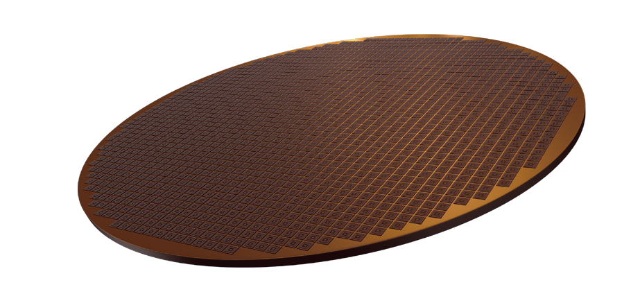
In the semiconductor market, where some argue that Moore’s Law is reaching its limit, the drive to implement extraordinary increases in functionality while diminishing – or maintaining – device dimensions is unabated. In order to achieve the desired footprints alongside cost/performance objectives, chip integration and new packaging approaches to functionality expansion are required. Fan-In Wafer-Level Packaging (FI WLP) and Fan-Out Wafer-Level Packaging (FO WLP) are two approaches that are showing promising cost efficiency and performance benefits as indicated by their market growth. According to market analyst, Yole Development, the CAGR from 2016 – 2022 for FO WLP is 31%, while FI WLP is projected to see 8% growth in the same period. For applications like data processors, mobile devices and automotive industrial systems, advancement of these technologies is good news. FO WLP is an extension of standard wafer-level packaging (WLP), but one that enables more I/O connections without having to increase the die size, allowing for a smaller package footprint with improved thermal and electrical performance. The process flow for FO WLP as compared to traditional WLP, where integrated circuits are packaged while they are still part of the wafer, is different. In FO WLP processing, the wafer is diced first and the dies are then placed onto a carrier, which is then compression molded. A redistribution layer is made on top of the entire molded area, following which solder balls are mounted onto the top.
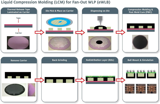
Figure 1: FO WLP process flow (chip-first, die face-down).
Alternatively, FI WLP is a technology in which an integrated circuit is packaged at the wafer level as opposed to the fan-out approach of assembling various dies into a package after wafer dicing. The FI WLP approach is suitable for packaging dies with low input-output (I/O) counts. With this technique, a redistribution layer is used to connect copper pillars or bumps/balls on top of the die surface. Trenches are cut in between the individual dies, then filled with molding material to offer device protection prior to grinding and dicing into single units.
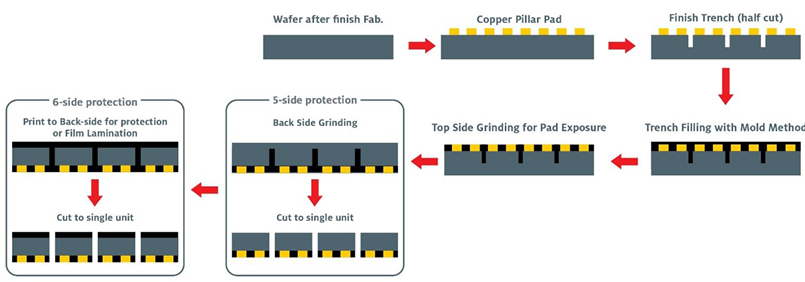
Figure 2: FI WLP process flow.
The Role and Evolution of Liquid Compression Molding for WLP Technology
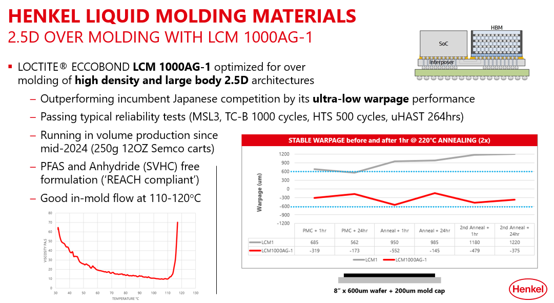
For both technologies, molding or encapsulation materials are essential, but serve different purposes. In the case of FO WLP, the compression molding step is where liquid molding materials are used to coat the dies on the reconstituted wafer. The encapsulating material –or liquid compression molding (LCM) material -- is critical for both handling to enable subsequent process steps and also to protect against warpage. With thinner dies – some as thin as 50 µm– the risk of warpage and, therefore, damage is large. LCM materials help reduce or eliminate that risk. For FI WLP devices, five- or six-side protection of the dies is necessary. This is achieved by filling the cut trenches with molding material to encapsulate all four sides and the die top with protective material prior to singulation. This protective layer prevents processing damage and enhances reliability during assembly. Until recently, the LCM materials widely available on the market were very granular or powder-type materials with large fillers (25 µm – 50 µm upper cut) built on anhydride resin platforms. In many cases, the materials resulted in high wafer warpage after molding which may ultimately lead to downstream wafer handling issues. Ideally, warpage should be kept to < 1 mm throughout the process. Secondly, the larger filler sizes of the granular LCMs prevent effective coverage and penetration between dies. The high-density nature of FI WLP and FO WLP technology makes the use of larger filler packages problematic. In order for materials to provide thorough encapsulation, fine fillers (average size 3 µm, with upper cuts at 10 µm) are desirable. Finally, while anhydride chemistry is effective, certain anhydrides are banned under the guidelines of the EU REACH legislation, identifying them as substances of very high concern (SVHCs) that could potentially be a supply chain risk if used in LCM formulations. With these realities as the backdrop, a team of chemistry specialists began the development of a new line of encapsulants that would overcome current challenges for liquid compression molding processes and enable higher reliability FO WLP and FI WLP devices. The result is a novel LCM formulation, LOCTITE ECCOBOND LCM 1000AG-1, built on a REACH-compliant, anhydride-free resin platform which has led to improved properties as they relate to warpage control, gap filling and in-mold curing. The material can be used for both FI WLPs and FO WLPs according to the process flows shown in Figures 1 and 2 above. Henkel’s new anhydride-free platform has shown significant improvements in:
Warpage Control
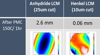
After curing, an 8” wafer coated with the Henkel LCM showed < 1.0 mm warpage versus 2.6 mm warpage with the anhydride LCM material. The platform can be modified for different applications, while maintaining ultra-low warpage control.
Fine Gap Filling
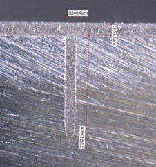
Because of the fine filler particles used in the new Henkel LCM, fast flow rates and void-free trench filling and underfilling is achieved, leading to more complete coverage, protection and long-term reliability. A trench measuring 40 µm in width by 400 µm in depth is completely filled with no voids using the next generation LCM material.
High Throughput Process
With a five-minute in-mold cure time versus an average ten-minute cure time for anhydride-based LCM encapsulants, the Henkel’s LOCTITE ECCOBOND LCM 1000AG-1 material allows advanced packaging specialists to more than double throughput and accelerate UPH.
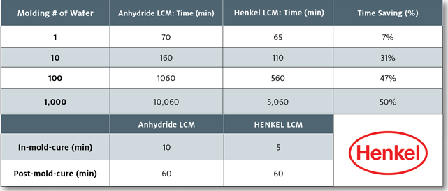
Figure 3: Henkel’s LCM material significantly improves throughput.
As FO WLP and FI WLP devices are increasingly incorporated into electronic systems to satisfy footprint/cost/performance expectations, materials like Henkel’s latest LCM innovation will be required to ensure reliability and enduring function. To learn more, visit Henkel Adhesives or contact us.
Recommended Cure Schedule
- 10 min @120°C (In mold cure)
- 1 hour @150°C (Post mold cure)