Flip Chip CSP
Flip chip means flipping over the chip to connect with the substrate or leadframe. Flip chip uses solder or bumps like copper pillar for interconnection other than conventional wire bonding. The I/O pads can be distributed all over the surface of the chip, thus the chip size can be shrunk with an optimized circuit path. The absence of a bonding wire also help reduce signal inductance. The key features of Flip Chip packages:
- Enhanced electrical performance. It provides a shorter path between die and substrate and eliminates the z-height impact of wire bond loops.
- Increased routing/signal density with small size. Coupled with copper pillar bumped die, flip chip technology could reduce layer count and cost applying fine line/space substrate routing and bump pitch.
- High Manufacture Efficiency. The package is processed in a strip format and all the bonding is completed in one process wafer bumping.
- Direct Heat dissipation path. An integrated heat spreader and external heat sink can be directly applied to remove heat.

FCCSP (Flip Chip Chip Scale Package) offers chip scale capacity for I/Os around 200 or less. FCCSP provides better protection for chip and better solder joint reliability compared with direct chip attach (DCA) or chip on board (COB). FCCSP features thin and small profile, and lightweight packages.

- Suitable for low and high-frequency applications
- Electroplated Pb-free or Cu pillar bumps
- Coreless, thin core, laminate, and molded substrate construction
- Bare die, over-molded, exposed die molded constructions
- Molded underfill (MUF) or Capillary underfill (CUF) options
- BGA ball pitches down to 0.1 mm scale
- Bump pitches with Cu pillar down to 0.01mm scale
- Package thicknesses down to 0.35 mm
- Accommodates package sizes from 1×1 mm2 to 25×25 mm2
- Heat spreader attach available for high-power devices
- Bottom-side chip attach available for Antenna in Package (AiP) applications
- Mobile processor (smart phones, tablet, wearable electronics); consumer and automotive.
- Chipsets for peripheral IC, RF, PMIC, Sensors/MEMS, connectivity
- Moisture Sensitivity Level: JEDEC Level 3@260°C
- Temperature Cycling Test: -55°C/125°C, 1000 cycles
- High Temperature Storage: 150°C, 1000hrs
- Highly Accelerated Stress Test: 130°C, 85%RH, 2 atm, 96 hrs
The above are typical condition numbers.

Overmold For FCCSP
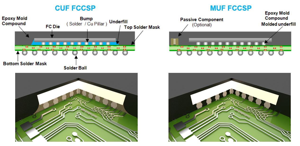
There are two ways of overmolding for FCCSP. One is using capillary underfills (CUF), the other one is using epoxy molding compound to substitute underfill (MUF) for lower cost, improve the thermal performance and 2nd level reliability.

| Product Recommendation For FCCSP Overmolding | ||
| Semicondutor Capillary Underfill (CUF) | Board Level Underfill | Epoxy Molding Compound Mold Underfill (MUF) |
UF8828 FP4511 FP4549 (HT) | Hysol GR920 Series | |
|
|
|
Mold Underfill Epoxy Molding Compound GR920
| Property / Product | Unit of Measure | Hysol GR920 H4 | Hysol GR920 Q2 | Hysol GR910 M12 | Hysol GR910 L20 | Hysol GR920 A1 |
|---|---|---|---|---|---|---|
| UNCURED PROPERTIES | ||||||
| Epoxy Type | MAR | MAR/MF | MAR/BP | MAR/MF | BP | |
| Hardener Type | MAR | MAR/MF | MAR | MAR/MF | PN/MF | |
| Filler cut | µm | 20 | 20 | 20 | 20 | 20 |
| Filler content | % | 84 | 85 | 88.5 | 88 | 87.5 |
| Filler Type | Spherical | Spherical | Spherical | Spherical | Spherical | |
| Hot Plate Gel time, @ 175°C | s | 34 | 39 | 37 | 34 | 46 |
| Spiral Flow @ 175°C | inch | 60 | 56 | 39 | 36 | 66 |
| Halogen-free (Green) | ✔ | ✔ | ✔ | ✔ | ✔ | |
| TYPICAL CURED PROPERTIES | ||||||
| Glass Transition Temperature, TMA | °C | 102 | 138 | 120 | 158 | 150 |
| Coefficient of Thermal Expansion (CTE) | ||||||
| Alpha1, TMA | ppm/°C | 14 | 12 | 10 | 9 | 9 |
| Alpha2, TMA | ppm/°C | 43 | 45 | 35 | 33 | 34 |
| Glass Transition Temperature, DMA | °C | 113 | 146 | 127 | 156 | 151 |
| Flexural Strength @25°C | MPa | 125 | 146 | 120 | 154 | 138 |
| Flexural Modulus @25°C | MPa | 13500 | 15500 | 19500 | 17800 | 24000 |
| Modulus by DMA @25°C | Mpa | 21000 | 20700 | 24000 | 25914 | 24000 |
| Modulus by DMA @175°C | Mpa | 350 | 1200 | 950 | 2119 | 2000 |
| Modulus by DMA @260°C | Mpa | 235 | 650 | 650 | 1203 | 1100 |
| Water Absorption, 24hr PCT | % | - | - | - | 0.37 | 0.38 |
| Mold Shrinkage PMC | % | 0.36 | 0.26 | 0.13 | 0.20 | 0.19 |
| Shore D Hardness | - | 76 | 77 | 76 | 81 | 80 |
Board-Level Underfills for CSP
They are used for mechanical reinforcement and to improve the thermal cycling performance. These underfills are used to absorb the CTE mismatch between the die and the substrate the die is placed on. They increase the reliability by distributing stress across the surface of the die or the substrate instead of being concentrated in the solder balls, especially during thermal cycling.
There are three main underfill types:
1. Capillary Underfill
- Dispense material along edge(s), completely flows under the component and fills the complete space
- Improved thermal and mechanical reliability
2. Partial Underfill - Corner Bond
- Dispensed before reflow
- Dispense dots or “L” shape only at the corners
- Small improvement in mechanical reliability, not in thermal reliability
3. Partial Underfill - Edge Bond
- Dispense after reflow
- Only covers corner fillets
- Small improvement in mechanical reliability, not in thermal reliability
- Can be UV or thermal Cure
Recommended products:
CUF (Capillary)
- UF8830S,
- UF8828,
- FP4511,
- FP4549(HT),
NCP (Pre-Applied)
- FP5201,
- NCP5209


