
Transistors
MOSFETS, TOS and BJTS
- Home

- Semiconductors
- Transistors
- Insulated-Gate Bipolar Transistor (IGBT)
Insulated-Gate Bipolar Transistor (IGBT)
Insulated-Gate Bipolar Transistor (IGBT) is a power semiconductor device that blends the strengths of two well-established technologies: the MOSFET, known for its fast switching speed, and the BJT, valued for its low conduction loss at high current. This hybrid design allows IGBTs to handle voltages ranging from 600 V to 6.5 kV while delivering both efficiency and controllability. In simple terms, you can think of an IGBT as the torque of a diesel engine (BJT efficiency) combined with the responsiveness of a sports car (MOSFET speed).
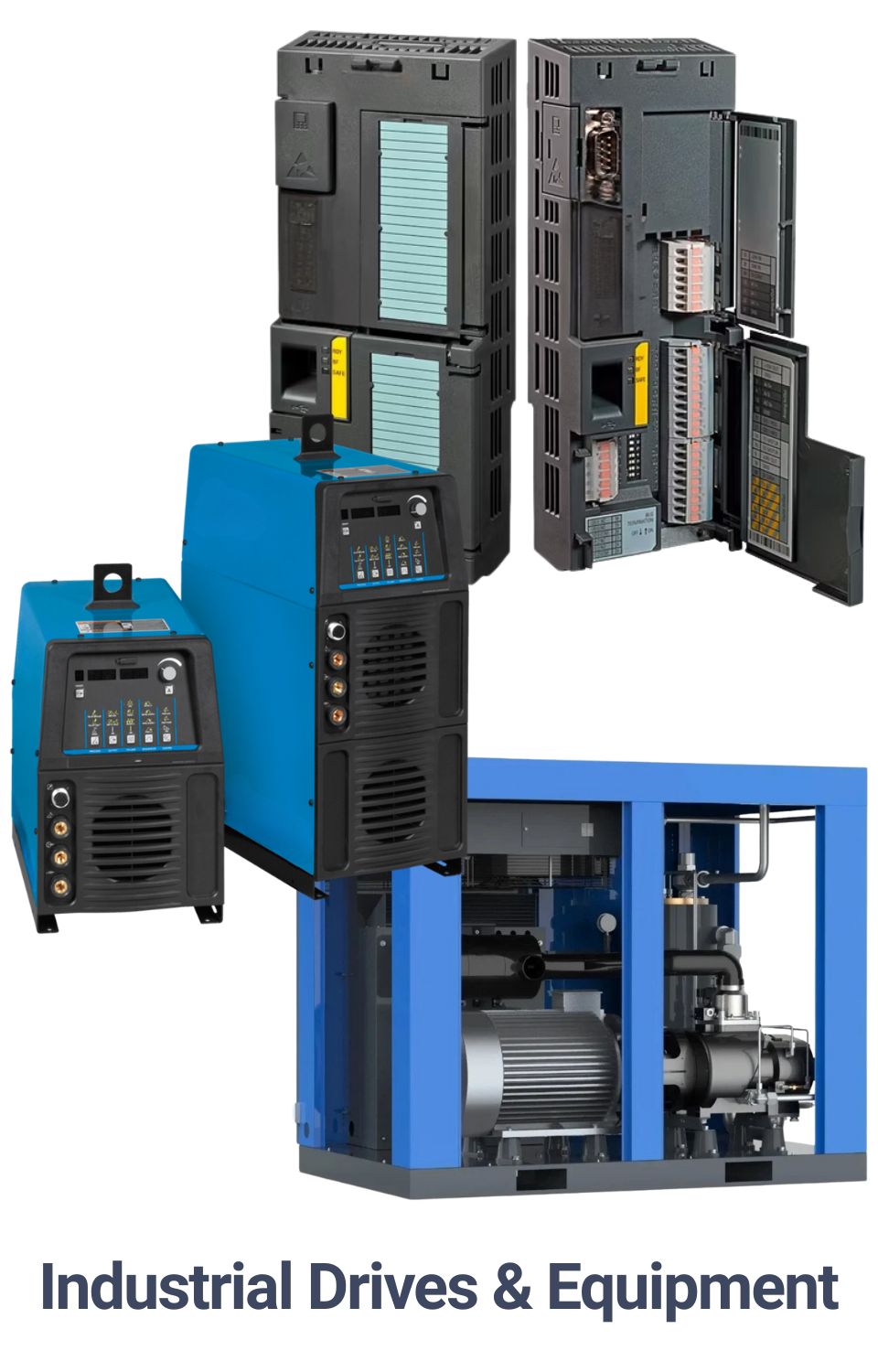
In systems like inverters, motor drives, renewable-energy converters, UPS, chargers, and welding equipment, an Insulated-Gate Bipolar Transistor (IGBT) is used to switch and control high voltage and high current efficiently in power electronics. Its purpose is to convert and regulate power. By combining MOSFET-style gate control with BJT-level conduction, an IGBT enables compact, efficient, and reliable high-power designs.
When comparing IGBTs and MOSFETs, the operating range becomes clear. IGBTs excel in high-voltage, medium-frequency applications, making them ideal for industrial and automotive power systems. MOSFETs, on the other hand, dominate lower-voltage, high-frequency applications, where switching speed is more critical than conduction efficiency. BJTs, though less common today, remain relevant in certain low-frequency, high-current applications.
The advantages of IGBTs are well recognized: they exhibit lower conduction losses than MOSFETs at high current, offer higher current density with simpler gate drive than BJTs, and provide a wide Safe Operating Area (SOA) with rugged performance. At the same time, they are not without limitations. Switching tail current (Eoff) can raise turn-off losses, and there is a risk of latch-up if the internal parasitic thyristor is unintentionally activated.
 Source: chargedevs.com
Power Device Comparison
| Device | Key Strength | Limitation | Typical Use |
|---|---|---|---|
| MOSFET | High switching speed | Higher conduction loss | Low-to-medium power, high-frequency circuits |
| BJT | Low conduction loss | Slower switching | Low frequency, high current applications |
| IGBT | MOSFET speed + BJT efficiency | Not ideal for very high frequencies | Medium-to-high voltage: EVs, drives, renewable inverters |
Despite these drawbacks, IGBTs remain the workhorse of medium-to-high voltage power electronics. They are widely used in EV traction inverters, renewable energy converters, industrial motor drives, welding equipment, UPS systems, and high-power charging solutions. For applications requiring very high-frequency switching beyond 50–100 kHz, however, SiC MOSFETs and GaN HEMTs are the devices of choice.
See also: SiC & GaN Power Devices Page
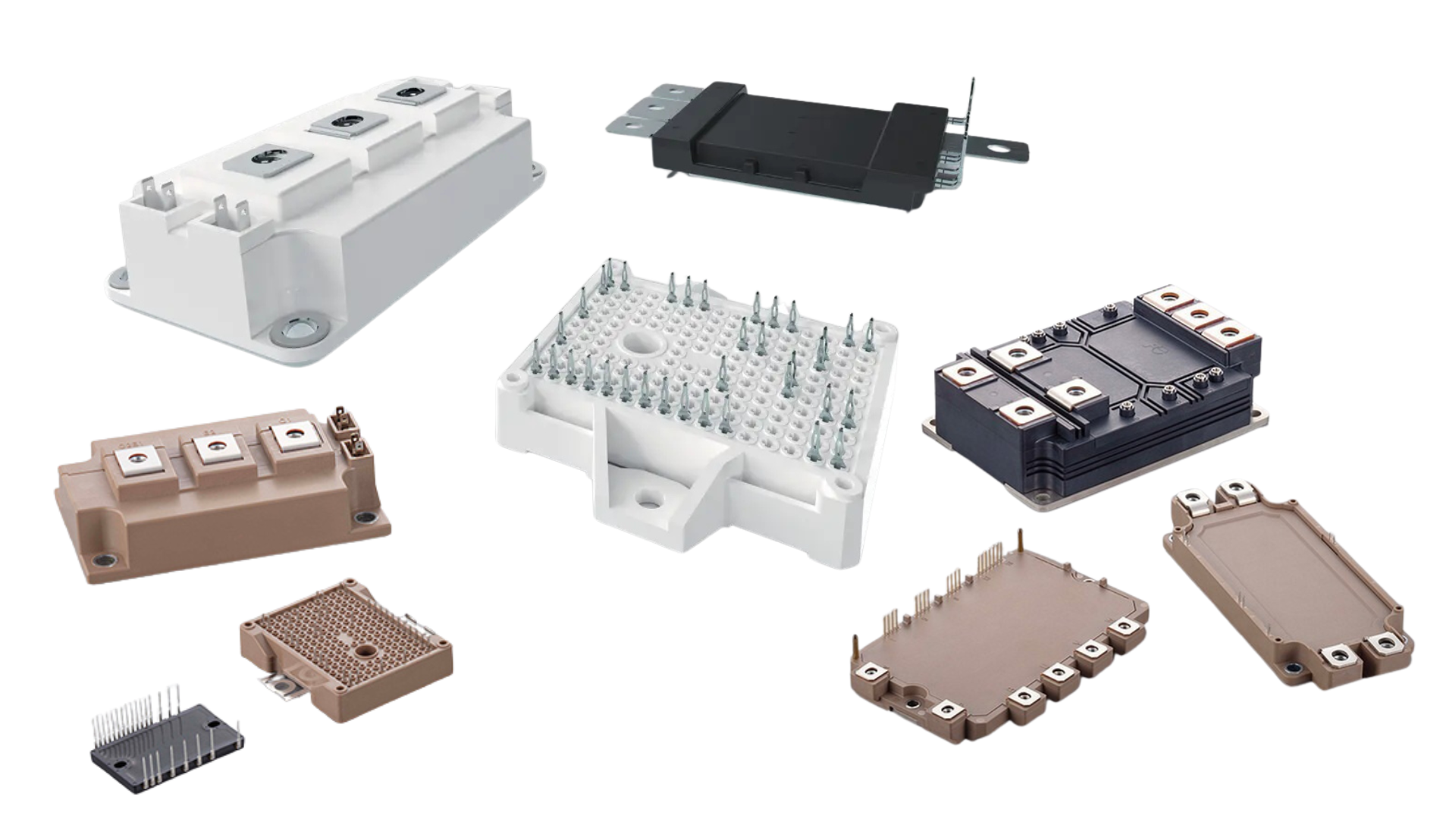
Types of IGBT Packages
Insulated-Gate Bipolar Transistor (IGBT) in different systems is generally divided into two formats: discrete and module.
IGBT Discrete
Discrete IGBTs are single-device power switches used when designs need high voltage and current in a compact, replaceable package. They come in through-hole (heatsink-mounted) and SMT (reflow-soldered) formats covering ~600–1200 V. Typical targets include motor drives, welders, UPS/PFC stages, chargers, tools, and industrial power supplies.
- Through-hole (TO-247, TO-220, TO-3P)
Built for strong cooling via a bolt-down tab and thermal interface material (TIM). Preferred when continuous current, low thermal resistance, and easy field service matter. - SMT (TO-263/D²PAK, TO-252/DPAK, SOT-223/457)
Optimized for automated assembly and tight layouts, using PCB copper planes and vias for heat spreading. Ideal for space-constrained, high-volume products at low–mid power.
Most Common Type: TO-247 (600–1200 V)
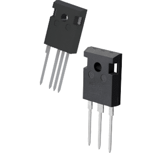
TO-247 IGBT offers a large die area, sturdy creepage/clearance, and a direct heatsink path for reliable thermal performance. It balances conduction loss and switching speed well for the 2–20 kHz range common in inverters and drives. It’s a go-to choice for industrial motor drives, EV chargers, welders, and UPS inverters.
PROs: High current capability, strong thermal path, easy service.
CONs: Bigger footprint/height, manual mounting, higher lead inductance than SMT.
USE CASES: Motor drives, welding power sources, UPS/PFC, chargers, industrial inverters.
IGBT Module
IGBT Power modules integrate multiple IGBT dies, freewheel diodes, and sensing into one block to deliver high power density and simplified assembly. Common styles include standard baseplate, baseplate-less, transfer-molded (TMPM), and double-sided cooling. Typical stacks use DBC ceramics (Al₂O₃, AlN, Si₃N₄) for isolation and heat spreading across half-bridge, six-pack (3-phase), chopper, and 3-level NPC/T-type topologies.
- Standard baseplate: DBC on a metal baseplate for flat mounting and strong heat spread—common in industrial drives, PV/wind inverters, and large UPS.
- Baseplate-less: No baseplate to cut thermal resistance and weight—ideal for compact, high-volume builds and automotive traction.
- Transfer-molded (TMPM): Overmolded die and interconnects for sealed, rugged, moisture-resistant modules—suited to harsh, high-vibration use.
- Double-sided cooling: Cooled from top and bottom to reduce thermal gradients—maximum power density and lifetime with more complex cooling.
Most Common Type: Standard baseplate six-pack (3-phase)
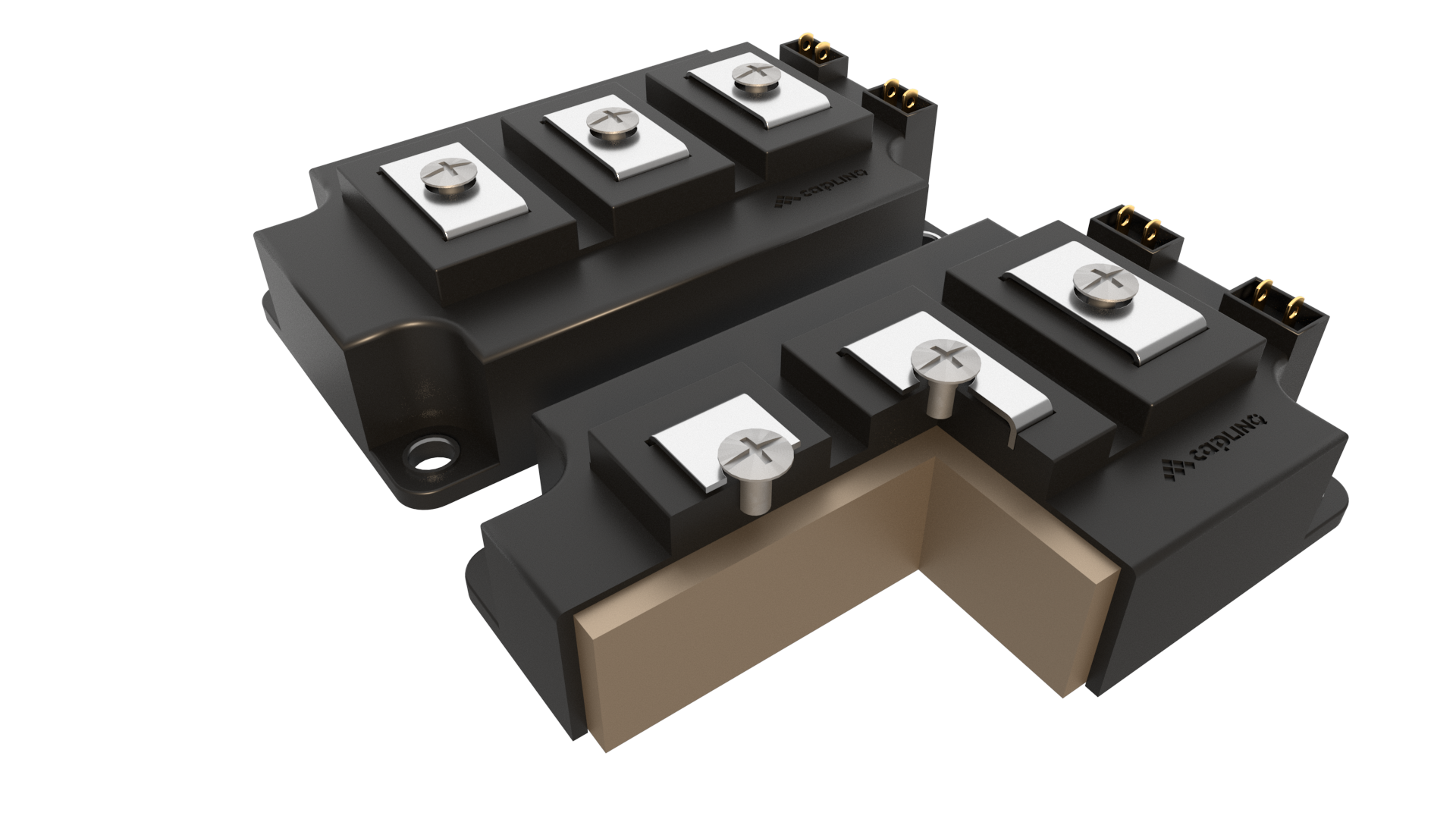
Six-pack baseplate module integrates three half-bridges in one package for compact 3-phase inverters. It offers proven mechanics, broad supplier availability, and straightforward heatsink or cold-plate mounting. It’s widely deployed in industrial drives, PV/wind inverters, elevators, compressors, and large UPS.
PROs: Robust mounting, good thermal spreading, easy system integration.
CONs: Higher mass/height, extra interface adds some thermal resistance.
USE CASES: 3-phase motor drives, renewable-energy inverters, large UPS/PFC systems, general-purpose high-power converters.
IGBT in Power Electronics
1) High efficiency at high power
- Low voltage drop when “on” → less energy wasted as heat.
- Result: smaller heatsinks, higher power density, better overall efficiency in big systems like EV inverters and factory drives.
2) Fast, clean switching (right where industry runs)
- Works best in the ~2–20 kHz switching range common to motor drives, traction inverters, UPS, and PFC stages.
- Voltage-controlled gate (easy to drive) and standard snubber/diode choices make switching predictable and repeatable.
3) Built for reliability and tough conditions
- Designed to survive short circuits, turn-off spikes, and inductive loads.
- Modern packaging and materials (robust substrates and die attach methods) help IGBT modules last through heat, vibration, and long duty cycles, meeting industrial and automotive standards.
![[IGBT Application Scope]](https://images.caplinq.com/applications/0199604ae0c277d68c4233277d9d1e0a-blobid0.png)
IGBT in Different Applications
IGBTs occupy the sweet spot for medium-to-high voltage and high current where efficiency under load, controllable switching, and cost matter more than extreme switching frequency. That’s why they dominate EV traction inverters, renewable-energy converters, industrial drives, welding systems, and large UPS/charger platforms. Where frequency rises significantly or partial-load efficiency is paramount at high bus voltages, SiC/GaN increasingly take the lead; otherwise, IGBTs remain the practical, power-dense, and reliable choice.
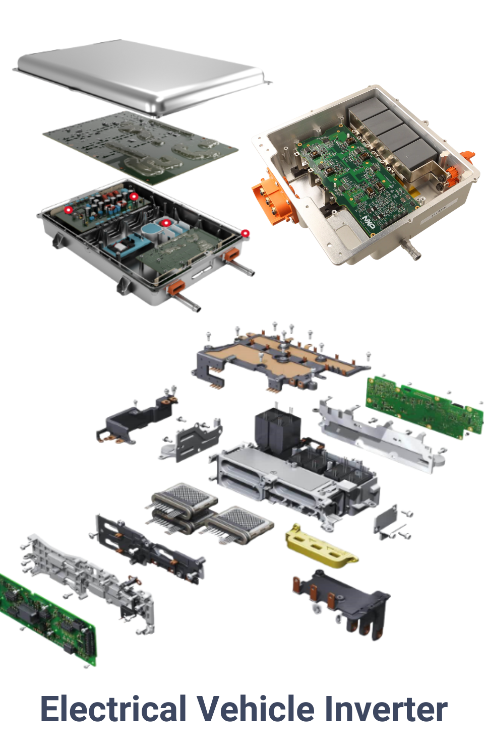
EV and HEV traction inverters (typically 400–800 V DC links, ~10–20 kHz) rely on IGBTs for low VCE(sat) at high torque and predictable switching at cruise/light load. Best-practice designs pair IGBTs with Kelvin emitter packages, laminated DC links (to suppress Lσ), tuned gate resistors for soft turn-off, and fast freewheel diodes (often SiC) to reduce Eon. With proper thermal paths (sintered Ag die attach, Si₃N₄ DBC, high-performance TIM), IGBT modules deliver high cycling endurance and low inverter losses across drive cycles.

In PV and wind converters, IGBTs form the backbone of DC/AC inverters and DC/DC stages, especially at 1.0–1.5 kV system voltages. Three-level topologies (NPC/T-type) let designers halve device stress and switching loss, pushing higher efficiency at moderate switching speeds. Wind turbine converters may use press-pack IGBTs for line-side robustness, while PV central and string inverters commonly adopt module IGBTs + SiC diodes for optimized Eon. IGBTs here balance efficiency, grid-code compliance, and lifecycle cost at utility scale.
Variable-frequency drives for pumps, compressors, conveyors, and robotics typically switch in the 2–8 kHz range where IGBTs offer excellent conduction efficiency, thermal robustness, and SOA. Their rugged short-circuit performance and predictable turn-off under inductive load make them the default in production environments. Welding power sources (with long output cables and punishing load steps) favor fast IGBT variants, tuned gate networks, and tailored snubbers to keep dv/dt and overshoot in check—delivering stable arcs, compact form factors, and long service life.
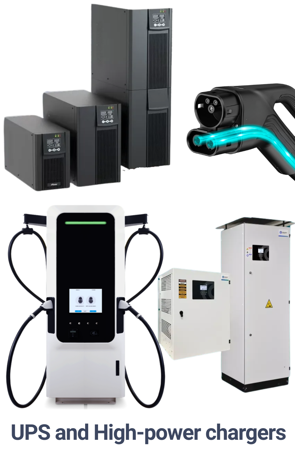
Double-conversion UPS systems (data centers, hospitals, industrial plants) use IGBT bridges for high-efficiency inversion and fast transfer with clean output waveforms under high crest-factor loads. Front-end PFC and fast DC chargers (depot/industrial) likewise rely on IGBTs for heavy RMS current handling and robust protection (desat + soft-off). Designs often mix IGBT power stages with SiC diodes to trim switching loss while preserving the IGBT’s favorable conduction profile at scale.
Other notable uses
- Rail traction & high-speed trains – IGBT traction inverters convert line DC/AC to multi-megawatt motor power with proven reliability and serviceability.
- Induction heating – IGBT arrays serve medium-frequency systems (tens of kHz) where power is high and MOSFET conduction loss would be excessive.
- SMPS & audio – At very high frequency, MOSFET/SiC typically win; IGBTs appear where bus voltage and current are high and switching frequency is moderate, e.g., specialized high-power SMPS or high-voltage Class-D stages.
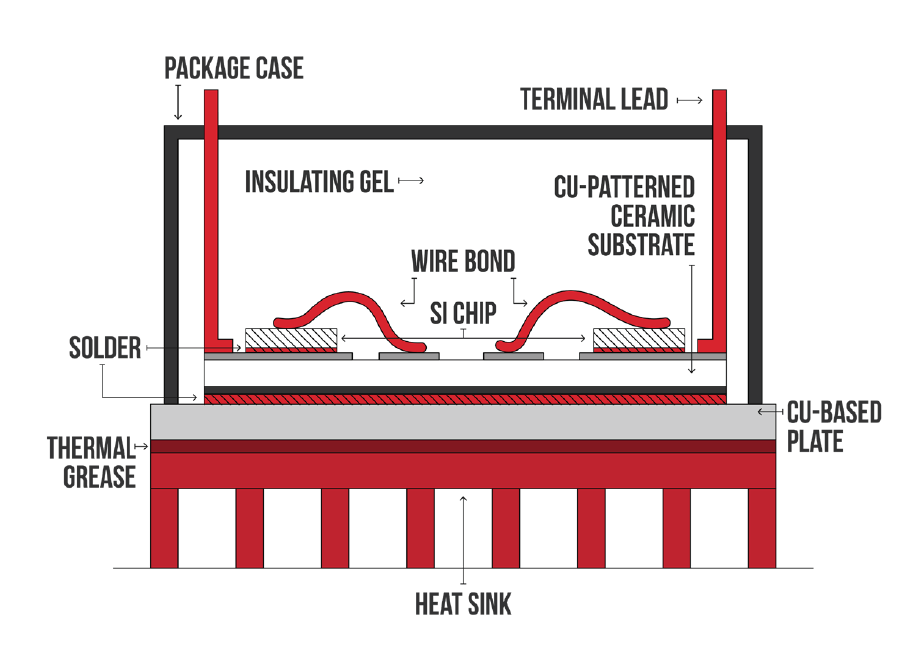
Key Challenges IGBT Packaging
IGBT modules succeed when heat is moved out, parts stay mechanically sound, insulation stays clean, and the assembly survives tough, real-world use.
Thermal
Some power always turns into heat while the device carries current and each time it switches. Use high-thermal-conductivity bonding and encapsulation with a thin, even bond layer to move heat fast.
Electrical
Impurities and trapped air pockets can create weak spots that leak current or spark at high voltage. Select low-impurity, solvent-free materials that cure clean and bond tightly, and design for low-void assembly
Mechanical
Different materials expand and contract at different rates, which can crack joints or warp layers over time. Choose conductive die attach and encapsulants with the right stiffness, and set bond-layer thickness to balance heat flow and stress
Harsh Reliability
Automotive and aerospace duty cycles demand steady operation at high temperature (about 175–220 °C), plus resistance to moisture, vibration, and long service life. Use automotive-grade materials, high-temperature molding compounds, silicone gels, advanced ceramic substrates, and durable thermal interface materials, then confirm performance with long-duration heat and power-cycling tests.
Materials for IGBT Packaging
Reliability is largely a materials-and-packaging achievement. IGBT packages must deliver strong heat flow, clean insulation, and mechanical durability to survive automotive and industrial duty. Core requirements include: low thermal resistance; steady performance at high temperature (≈175–220 °C); resistance to moisture, vibration, and long power/thermal cycling; low voids; low-ionic/clean chemistry; good adhesion; corrosion resistance; adequate creepage/clearance; manufacturability and inspection readiness.
Die Attach in IGBT Packages
Die attach creates the thermal, electrical, and mechanical link between the silicon die and the substrate; in IGBT packages, it must run hot and clean, with low voids and stable performance at elevated junction temperatures typical of automotive/industrial duty (≈175–250 °C). Today’s landscape: solder (SnAg, AuSn) and conductive epoxies are widely used—especially in discrete parts—while sintered silver has become common in high-power modules for its thermal and cycling advantages.
Solder-based Die Attach
- Mature & high-throughput manufacturing with established wetting/reflow practices; AuSn is widely used and can be processed flux-free, simplifying cleanliness.
- Good electrical/thermal conduction with proven reliability when joints are well-formed and microstructure is controlled.
- Broad material choices (Pb-free SAC, AuSn) to match melting range and process windows for discrete and module assembly.
Limitations: creep-fatigue · flux/residue cleanliness · lower thermal conductivity vs Ag-sinter · void control · remelt risk in multi-reflow · warpage/microstructure aging · RoHS constraints
Silver Sintering Die Attach
- Very high thermal conductivity and low thermal resistance joints, improving heat flow from die to DBC in high-power modules.
- High-temperature robustness & cycling life; widely adopted in modern IGBT modules (e.g., nano-Ag sinter on DBC).
- Strong mechanical/electrical properties with low voiding potential when processed correctly.
Limitations: noble-metal finish need (Ag/Au) · pressure/temperature process window · surface cleanliness/planarity sensitivity · higher material & tooling cost · limited reworkability · plating/supply chain dependency
Recommended Die Attach for IGBT Packaging
For IGBT Packaging die attach, we want:
- Low thermal resistance and stability at high junction temperatures (about 175–250 °C).
- Clean, low-void, well-adhered bonds validated by standard inspection/qualification practices.
- Finish/process compatibility with DBC/substrates (e.g., Au/Ag finishes for Ag-sinter; flux-free options for AuSn).
For both discrete IGBTs and power modules, materials must deliver low thermal resistance and stable high-temperature performance (≈175–250 °C), clean, low-void, well-adhered bonds, and finish/process compatibility with common DBC and leadframe surfaces (Au/Ag/Cu).
Featured Products
Solder-based Die Attach
ALPHA® High-Lead Die-Attach Solder Preforms ↗
4N-purity PbSn/PbSnAg/PbSb preforms in die-attach shapes (discs/squares), hermetically packed; supports high-temperature, forming-gas reflow for low-void, robust joints in IGBT discretes and modules.
- High-temp stability & strong heat conduction
- Compatible with Au/Ag/Cu finishes; wide size range
LINQALLOY SP-PSA525 (92.5Pb/2.5Ag/5Sn) ↗
High-lead no-clean solder paste engineered for die-attach dispensing; consistent deposits, strong joints, and good wetting for power-semiconductor assembly.
- Built for automated dispensing; low voiding
- Ideal for applications where post-soldering cleaning is unnecessary, providing minimal, non-conductive residues.
Silver-Filled Epoxy Die Attach
LOCTITE® ABLESTIK 84-1LMISR4 ↗
Silver-filled epoxy die-attach adhesive for high-throughput lines; heat-cure system widely adopted in power electronics.
- Clean dispensing; strong adhesion to metal/ceramic
- Can be applied by stamping, stencil or dispensing
LINQBOND™ DA-8030 ↗
Single-component, silver-filled die-attach adhesive with high thermal/electrical conductivity; bonds well to metal and ceramic.
- Low-temperature cure option; low voiding
- Designed for thin packages but can also be used for consumer electronics, automotive sensors, and diodes.
Silver Sintering Die Attach
LOCTITE® ABLESTIK SSP 2020 ↗
Silver sintering paste for high-heat-transfer power devices; maintains adhesion up to ~260 °C (Ag/Au-coated substrates).
- Ultra-low thermal resistance; lultra high thermal conductivity up to 200 W/mK
- Solvent based silver sintering material
LINQBOND™ DA-8060S (Pressure-less Silver Sinter) ↗
Pressure-less silver-sinter die-attach with high thermal conductivity and strong adhesion to Ag-spot, bare Cu, PPF, and ceramic substrates.
- Low-void bonds; built for IGBT module thermal paths
- provide exceptional thermal and electrical conductivity, ensuring efficient heat dissipation and reliable electrical connections
Encapsulation for IGBT Packaging
Encapsulation of discrete IGBTs and modules, similar to encapsulation in other semiconductor packages, is a critical step that ensures environmental protection, hermeticity, and long-term reliability. Encapsulation provides enough seal that prevents moisture, gas, or contaminant ingress, maintaining stable performance of IGBT in extreme industrial and automotive environments.
Encapsulation around die and interconnects to resist moisture, shock, and thermal cycling.
Why encapsulation matters
- Shields against environment: Encapsulation blocks moisture, dust, and chemicals, preventing corrosion and extending IGBT life.
- Strengthens & stabilizes: It absorbs stress from heat cycling and vibration, keeping chips, wires, and components secure and reliable.
- Insulates & cools: Encapsulation provides high-voltage insulation, manages electric fields, and helps transfer heat for safe operation.
Encapsulation for IGBTs is chosen by balancing electrical insulation, thermal stability, mechanical stress relief, environmental resistance, and process fit. Silicone gels suit high-voltage/PD resistance, epoxies give rigidity and high Tg, while filled systems improve heat spreading for demanding EV and industrial modules.
Featured Products
High Tg EMC for IGBT ↗
LINQSOL™ EMC-7535MF ↗
High-Tg, low-stress, halogen-free EMC for high-voltage / high-power discrete packages (e.g., TO-220, TO-247) and IGBT modules.
- Tg: 215 °C | CTI: 600 V | UL94: V-0
- Low moisture absorption; low ion content; reliable encapsulation for IGBT discretes and modules
HYSOL GR750 ↗
Halogen-free, silica-filled EMC with very high Tg for robust power packages and wide-bandgap devices.
- Tg: 235 °C | Low moisture absorption
- Excellent adhesion to Ni-plated leadframes; suitable for demanding power electronics
LINQSOL™ EMC-G374 ↗
Ultra-high-Tg EMC for high-power SiC / GaN and IGBT packages where temperature stability is critical.
- Ultra-high Tg class | High temperature stability
- Engineered for demanding high-power discrete and module encapsulation
Thermally Conductive EMC for IGBT ↗
LINQSOL™ EMC-G375 ↗
High-thermal-conductivity EMC for full-pack TO power packages and high-power rectifier packages.
- Thermal conductivity: up to ~3.3 W/m·K
- Built for heat-dissipation and long-term reliability in IGBT discretes
LINQSOL™ EMC-5013 ↗
Thermally conductive EMC for TO-220F, TO-3PF and full-pack power packages; insulative performance with low porosity.
- Thermal conductivity: >2 W/m·K | UL94 V-0 | Low water absorption
- Developed for high-performance power packages and IGBT discrete encapsulation
Dielectric Silicone Gels for IGBT↗
LINQBOND™ PM-4911HV ↗
Two-part, low-stress silicone gel for IGBT modules and discrete power devices. Mixes 1:1 and cures to a soft, clear gel that insulates, seals and damps vibration for long-life operation.
- Room-temperature; heat-accelerated optional
- Very low modulus; shock & moisture protection
- Potting/gel filling for IGBT modules & TO-packages
DOWSIL™ EG-4175↗
High-temperature dielectric silicone gel for next-gen IGBT modules. Self-priming adhesion and self-healing behavior help protect against thermal and mechanical stress.
- Room-temperature; heat-accelerated optional
- Designed for operation up to ~180 °C
- EV traction, PV/wind inverters, industrial power
Elantas Bectron® SG-75V1-15↗
Two-part silicone gel that cures at room temperature to a very soft, transparent encapsulant. Wide service range and excellent dielectric insulation for power electronics.
- RT cure (~24 h); heat-accelerated optional
- ~-45 °C to +200 °C
- Potting IGBT modules & sensitive power assemblies
Thermally Conductive Silicone Gel for IGBT ↗
LINQBOND™ PM-Si611 ↗
Two-part, thermally conductive silicone potting material for IGBT discretes and modules; designed for heat dissipation, electrical insulation, and reliable gel-like stress relief.
- Thermal Conductivity: >1.0 W/m·K
- Cure: 150 °C / 10 min or 100 °C / 60 min (fast-cure options)
- Hardness: Shore A 35 ± 5
- UL 94: V-0
DOW SYLGARD™ 170 ↗
Two-part silicone encapsulant/gel with moderate thermal conductivity and good flow for potting power electronics; suitable for heat-spreading and dielectric protection around IGBT assemblies.
- Thermal Conductivity: ~0.4 W/m·K
- Mix Ratio: 1:1; cures at room temp or with heat; low viscosity / good flow
- Flame-resistant, dielectric encapsulant for high-power electronics
Thermal Interface Materials IGBT Packaging
TIMs reduce contact resistance between the IGBT baseplate or discrete tab and the heatsink/cold plate, improving heat flow and cycling life. For both discretes (TO-220/TO-247) and power modules, prioritize a thin, uniform bondline under clamp load, resistance to pump-out/dry-out, and stability at elevated temperatures typical of automotive/industrial duty.
- Target metrics: low thermal impedance (°C·cm²/W), controlled bondline thickness (BLT), stable performance after power/thermal cycling.
- Fit for use: phase-change TIMs for tight flatness and lowest interface resistance; gap fillers/putties where tolerances/warpage demand conformity.
- Validation: clamp/BLT vs. torque, pump-out after cycling, long-term aging (150–175 °C), dielectric withstand (if required), and reworkability where needed.
Phase-Change TIMs
Honeywell PTM-6000HV↗
Printable/stencilable phase-change compound that forms a thin, low-impedance interface under clamp; designed for module baseplates and TO tabs.
- Low thermal impedance; resists pump-out/dry-out
- Forms uniform BLT under assembly pressure; reworkable
Honeywell PTM-7950-SP↗
High-viscosity PCM for low-mess printing and fast wet-out at operating temperature; tuned for repeated thermal cycling.
- Consistent deposition; thin BLT for low Rth
- RoHS compliant; serviceable interface
See more: Honeywell's Printing Process Guideline to IGBT ↗
Related Blogs
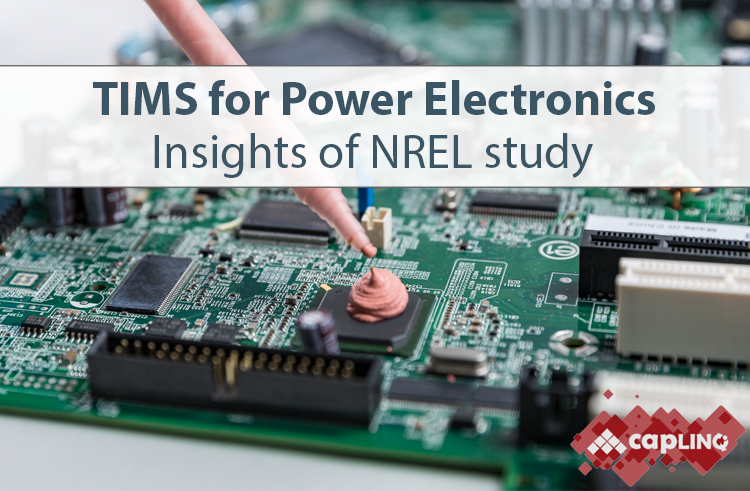
Thermal Interface Materials for Power Electronics: Insights from NREL Study
This blog summarizes an NREL study on Thermal Interface Materials (TIMs) for power electronics, focusing on their thermal performance, reliability, and cost. It evaluated 40 commercial TIMs, with Honeywell PCM 45G/PCM 45F showing the best results, achieving thermal resistance as low as <10 mm²K/W. The study highlights the importance of TIMs in automotive IGBT cooling and notes that while greases and gels are widely used, advanced materials like carbon nanotubes show potential.
You might also be interested in thermal solutions for inverters or TO packages for power modules.