Wafers
Wafer processing
- Home

- Semiconductors
- Wafers
Wafers
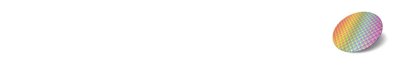
A wafer is the substrate used to create integrated circuits. It is the foundational building block of a semiconductor chip. It’s the very first component that kicks off the whole process. It’s called a wafer because once the individual dies are cut from it, it ends up looking like a round waffle—or, well, a wafer.
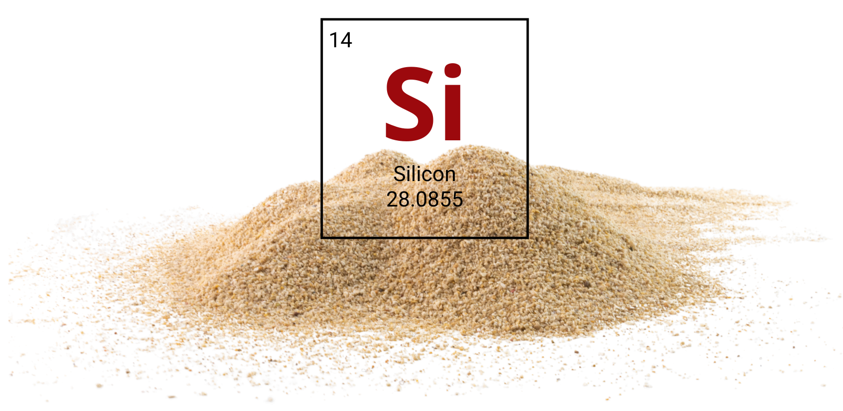
Wafers are made from a single element: Silicon (Si). In everyday life, you’ll recognize silicon in its raw form as sand. It’s one of the most abundant materials on Earth, which makes it a great (and affordable) starting point for building chips.
First and foremost, silicon is used because it’s easy to get your hands on. It’s one of the most accessible materials out there. But what really makes silicon ideal for use in wafer fabrication is that it’s a semiconductor. A semiconductor is a material that can either conduct electricity or resist it—depending on what’s needed. In simple terms, it can switch between acting as a conductor or an insulator, giving you the flexibility to use it in many electronic applications.
- Conductor - material which easily allows the flow of electricity
- Insulator - material which inhibits the flow of electricity
- Semiconductor - somewhere in between the two.
This quality makes the semiconductor an ideal medium to control electrical current and everyday electrical appliances. Semiconductors have properties that sit between the conductor and insulator. A diode, integrated circuit (IC) and transistor are all made from semiconductors.

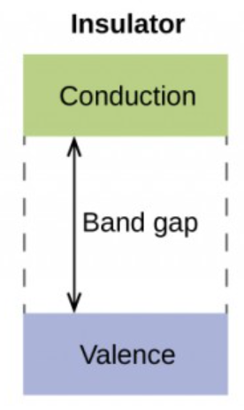
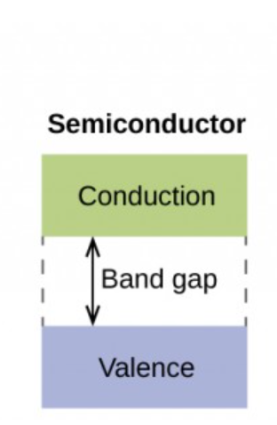
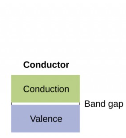
The reason that semiconductors behave this way in nature is because of the band gap. The band gap is a section in which no electronic states exist. It represents how far electrons have to travel to participate in conduction. So, as seen in the image below, insulators have a large band gap. This means the electrons have to travel very far to be able to conduct electricity. In conductors, the band gap is very small, allowing electrons to easily jump through the band. A semiconductor is the state described between the two.
How is a Wafer Made?
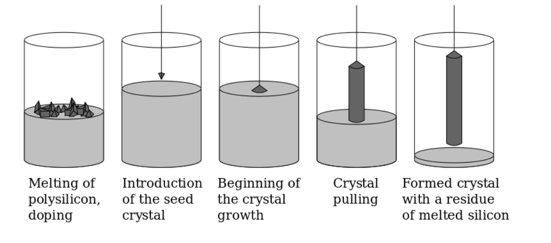
To make a wafer, the most common method is the Czochralski process. In this process, a single silicon crystal is grown into a large cylindrical ingot, which is then carefully sliced into thin, perfectly round wafers.
The wafer is the base on which all the intricate chip structures are built. Wafers are formed of highly pure, nearly defect-free single-crystalline material with a purity of 99.9999999% (9N) or higher. Mass production sizes are 4”, 6”, 8”, and 12 " wafer diameters.
Silicon Wafer Fabrication Process:
- Polycrystalline Silicon - High-purity silicon is produced in a polycrystalline form, to serve as the basis for wafer creation.
- Crystal Growth - A single crystal silicon ingot is grown through the Czochalski process.
- Single Crystal Silicon Ingot - Formed silicone crystal ingot
- Crystal Trimming and Grinding - the ends of the ingot are trimmed, and the surface is ground to an even diameter throughout the ingot
- Slicing - the ingot is sliced into thin wafers using slow-moving diamond-coated wire saws
- Edge Rounding - the edges of the wafers are ground to remove any sharp edges that might cause breakage during processing.
- Lapping - Flatness and thickness correction process, prepares the wafer for finer treatments.
- Etching (Chemical Polishing) - using abrasive materials like high purity alumina and mechanical grinding to polish the wafer to achieve extreme flatness.
- Polishing - finer version of No 8.
- Cleaning - Rigorous cleaning prior to inspection.
- Inspection - Checking for defects, flatness, quality, etc.
- Packing / Shipping - Preparation for shipping in specialized wafer packaging.
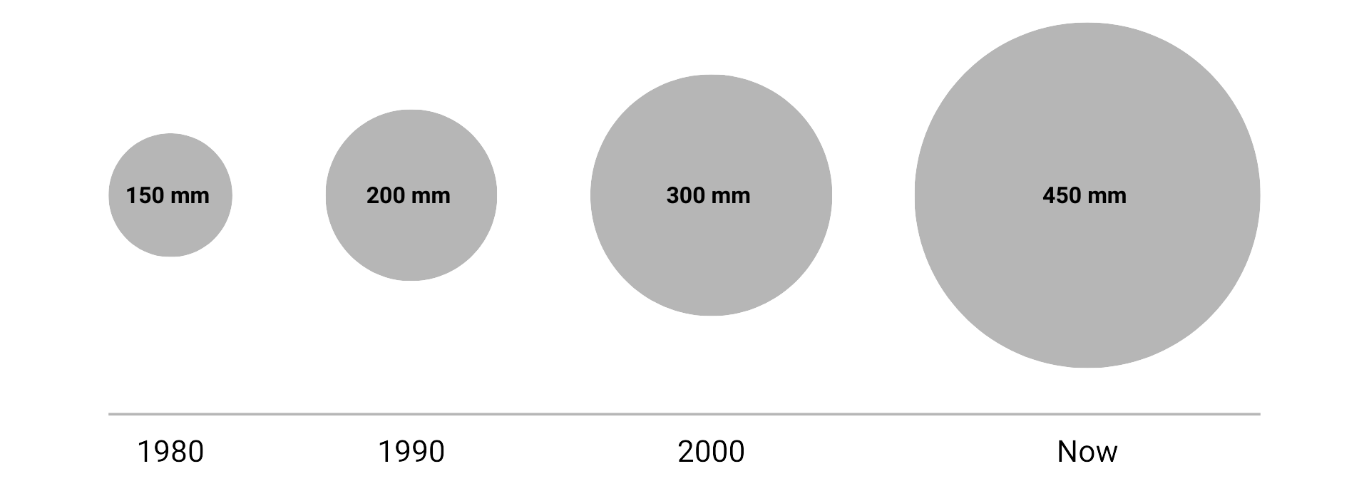
| Year | Size of Wafer (mm) |
| 1980 | 150 |
| 1991 | 200 |
| 2001 | 300 |
| Now | 450 |
Why Go Bigger?
The shift to larger wafer sizes is driven by the need to improve manufacturing efficiency and reduce the cost per chip. Larger wafers can hold significantly more dies, allowing more chips to be produced in a single processing run, which boosts throughput and lowers overall production costs. This also leads to better material utilization, as edge losses account for a smaller proportion of the wafer. While transitioning to larger wafers involves higher equipment costs and added challenges in handling and process control, the increased output and long-term cost savings make it a valuable move for high-volume semiconductor manufacturing.

Benefits of making larger wafers:
IMPROVES MANUFACTURING EFFICIENCY
Larger wafers increase chip production per run, improving throughput, reducing costs, and minimizing material waste from edge losses.
INCREASED CHIPS PER WAFER
Larger wafers can hold significantly more dies, allowing more chips to be produced in a single processing run.
Frequently Asked Questions about Wafers
LINQTAPE Dicing and Backgrinding Tapes
LINQTAPE Dicing and Backgrinding tapes are tapes specifically designed to be used in semiconductor and electronics manufacturing processes. These tapes feature a strong adhesive system designed for secure wafer handling during critical processes such as dicing and thinning. By utilizing high-performance materials with advanced adhesive properties, the tapes enhance both process efficiency and wafer yield, all while reducing the risk of damage during cutting and grinding operations.
⚡ Applications
▪ Die Cutting
▪ Masking
Temporary Bonding
Assembly of Delicate Components
✅ Advantages
✔ Strong Adhesion to prevent wafer damage
✔ Can be used with uneven surfaces
✔ High transparency, high and evenly distributed elasticity
📥 Downloads
⬇ Technical Data Sheet -
Backside Protection Film for Advanced Packaging Encapsulation
The traditional packaging process flow starts with dicing the wafer and then moving forward with the packaging. Wafer-level packaging skips these process steps by packaging everything while still on the wafer and then dicing individual, ready-to-go packages.
Benefits of LCM for WLP
VERY THIN WLP PACKAGES
ELIMINATES AIR VOIDS
The pressure during molding ensures good encapsulation and eliminates air voids, leading to high-density, reliable electronic components.
LOCTITE ABLESTIK BSP 125 Backside Protection Film
Shrinking dimensions and finer ball pitches in WLCSPs increase challenges like die chipping, wafer warpage, and damage during SMT placement. New film technologies, including backside protection (BSP) films, help reduce mechanical damage, improve laser marking, and enhance reliability. Additionally, low-warpage liquid compression molding compounds enable wafer-level chip packaging, paving the way for innovative IC packaging methods.
LOCTITE ABLESTIK BSP 125 is a black hybrid film is designed for WLCSP back side laser marking and chip protection applications. A package using this material will have an overall improvement in package reliability. It facilitates the production of highly miniaturized WLCSP devices, and exhibits high MSL reliability, low warpage and consistent bondline thickness. It is typically used for die attach in WLCSP applications as a controlled flow adhesive. It passes 1000 cycles TS-B testing and 168hours PCT.
⚡ Applications
▪ Die Attach
Wafer-Level Packaging
LED Bonding
Sensor and MEMS Packaging
✅ Advantages
✔ Excellent thermal stability up to up to 350°C without degradation
✔ High bonding stress which offers reliable adhesion and excellent mechanical stress
✔ Resistant to moisture, chemicals, and UV exposure
📥 Downloads
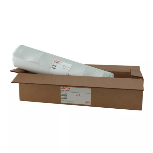
Wafer Backside Coatings for Wirebond Laminate and Leadframe Packaging
Wafer backside coating materials allow for screen or stencil printing of the paste across the entire wafer in a single stroke, increasing throughput by eliminating the need to individually dispense dots of adhesive.
liable electronic components.
LOCTITE ABLESTIK 8008 Backside Coating
Shrinking dimensions and finer ball pitches in WLCSPs increase challenges like die chipping, wafer warpage, and damage during SMT placement. New film technologies, including backside protection (BSP) films, help reduce mechanical damage, improve laser marking, and enhance reliability. Additionally, low-warpage liquid compression molding compounds enable wafer-level chip packaging, paving the way for innovative IC packaging methods.
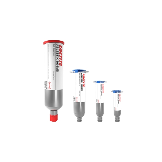
LOCTITE ABLESTIK 8008MD adhesive is designed for medium die attach applications. This thermally and electrically conductive proprietary hybrid product can be applied to a wafer backside by stencil printing and then B-staged in an oven.
LOCTITE ABLESTIK 8008MD can then be cured after die attach in an in-line process. This material has good substrate wetting, controlled bondline thickness was originally known as RP-825-3C1. It is typically used on PPF, Copper and Silver plated CU leadframes.
⚡ Applications
▪ Die Attach
Wafer backside coating
Advance packaging applications
✅ Advantages
✔ Superior adhesion providing excellent bond strength
✔ Low modulus which ensures flexibility and reduces stress
✔ Stencil printing compatibility
📥 Downloads
Frequently Asked Questions about [Application Name]
Presentations
CAPLINQ Materials for Alkaline Water Electrolyzers
This presentation provides an overview of CAPLINQ materials for alkaline water electrolyzers, focusing on their basic properties and performance. We will cover key material characteristics that make them suitable for enhancing electrolyzer efficiency and durability.
Related Blogs
CAPLINQ Polyimide Tape used to Sputter Metals on Wafers
This blog explores how CAPLINQ Polyimide Tape is used during the sputtering process of metals onto semiconductor wafers. It highlights the tape’s ability to withstand high temperatures and harsh chemical environments, making it ideal for masking and protecting wafer areas during metal deposition. It touches on the tape’s clean removability, precision, and reliability in microelectronics and semiconductor fabrication.
Same Size Die Stacking | Wafer Back Side Coating (WBC) Options
This blog explores Same Size Die Stacking and the role of Wafer Back Side Coating (WBC) in the process. It discusses how WBC enhances die protection, electrical insulation, and thermal performance, which are critical in high-density packaging. The article outlines different WBC material options and their impact on stacking yield, reliability, and process compatibility, helping manufacturers choose the right coating solution for advanced semiconductor applications.
Low-Stress Dielectric Layers for Wafer Level Packages to Reduce Wafer Warpage and Improve Board-Level Temperature-Cycle Reliability
This blog discusses the use of low-stress dielectric layers in wafer-level packaging (WLP) to address challenges like wafer warpage and board-level reliability during temperature cycling. It explains how selecting the right dielectric materials can minimize mechanical stress on the wafer, leading to better dimensional stability, improved package flatness, and enhanced thermal cycling performance—key factors for ensuring long-term reliability in advanced electronic assemblies.